At the Speed of GaN (gallium nitride)
![27_Pdf_File_Type_Adobe_logo_logos-512[1]](https://navitassemi.com/wp-content/uploads/2020/12/27_Pdf_File_Type_Adobe_logo_logos-5121.png)



At the Speed of GaN
Center for Power Electronics Systems
Annual Meeting April 2017
Gene Sheridan, CEO
[email protected]
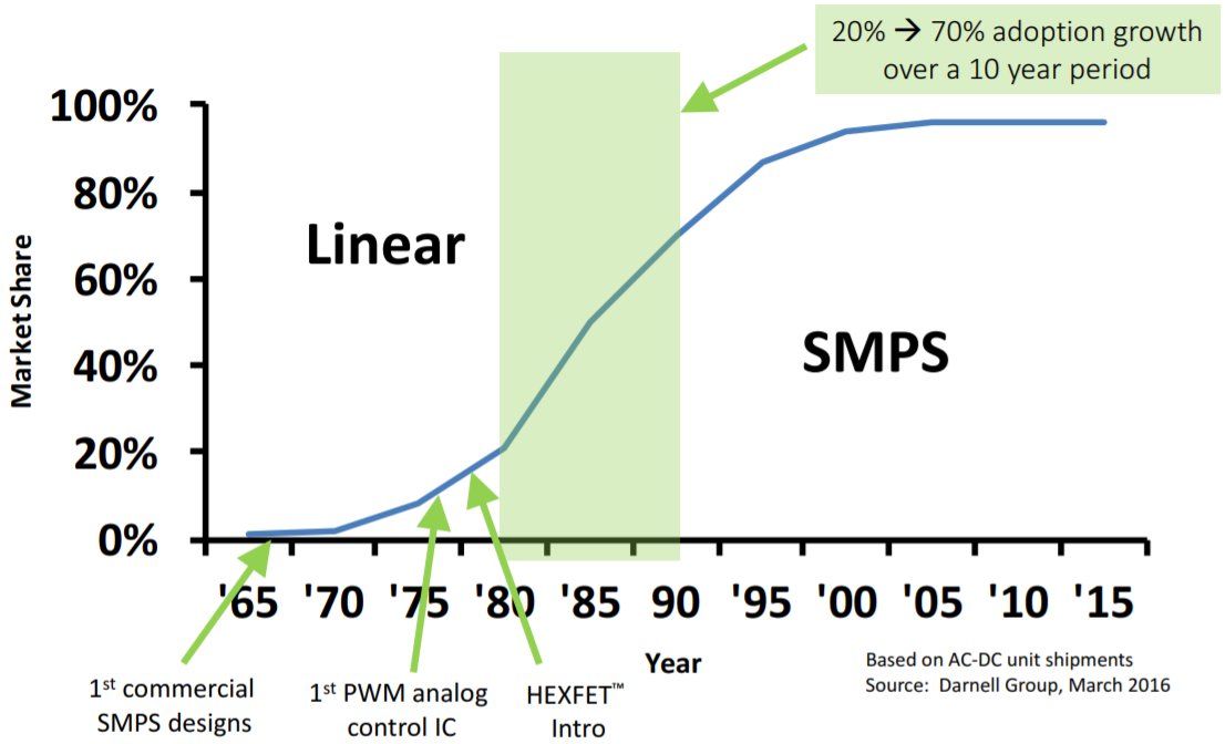
Linear vs. Switching Regulator Adoption
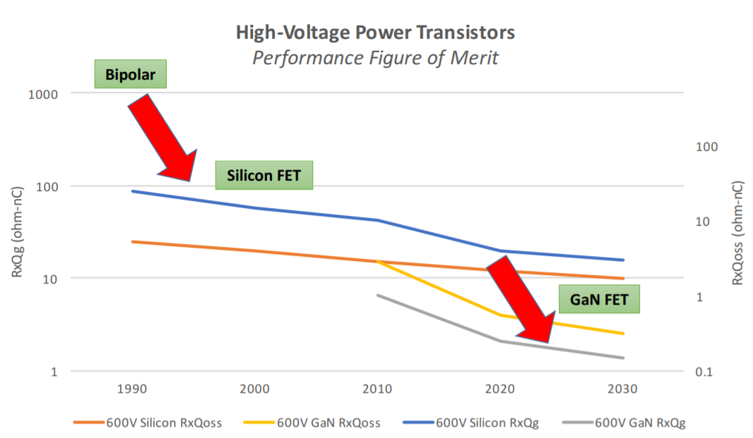
Power Transistors – 10x Disruptions
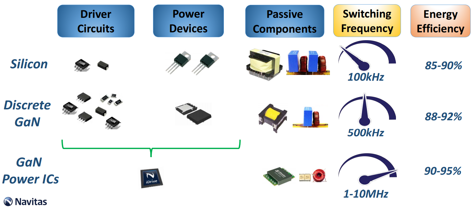
The Power of GaN Power ICs
… Unequaled Speed & Efficiency
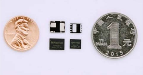
650V Half-Bridge AllGaN™ Power IC
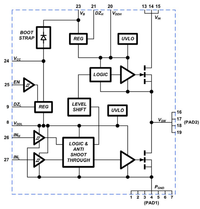
• Proprietary AllGaN™ technology
• Monolithic integration of 650V eMode GaN FET, driver, logic
• Internal level-shift & bootstrap circuits
• Ground-referenced, digital input
• High dV/dt immunity (200 V/ns)
• Zero inductance turn-off loops
• ESD, UVLO, shoot-through protection
• Flexible topologies: Active Clamp Flyback, Half-Bridge, LLC, etc.
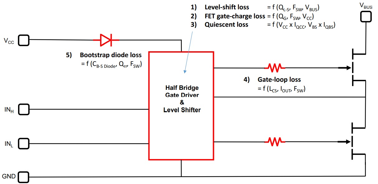
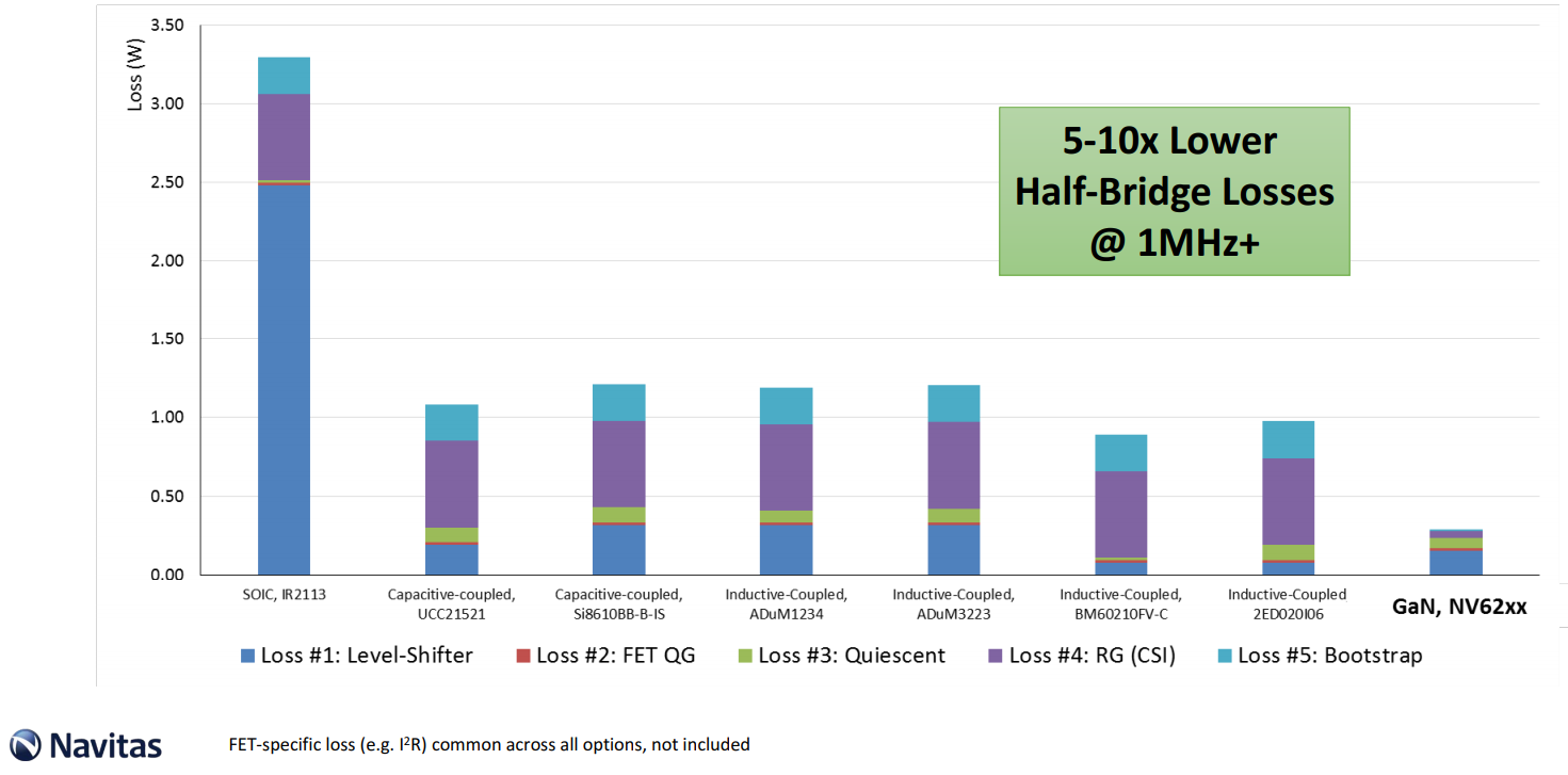
Discrete Half-Bridge Drive – 5 Key Losses
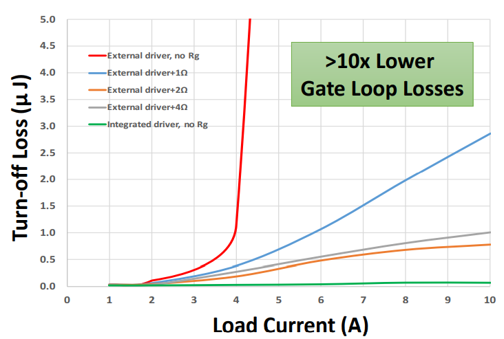
Eliminating Gate Loop Losses
External drivers
• Just 1-2 nH of gate loop inductance can cause unintended turn-on
• Gate resistors reduce spikes but create additional losses
Integrated GaN drivers (iDrive™)
• Eliminate the problem
• Negligible turn-off losses

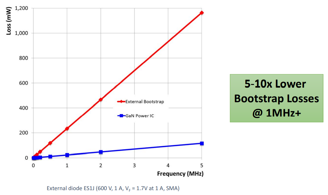
Eliminating Bootstrap Losses
Eliminating Half-Bridge Losses
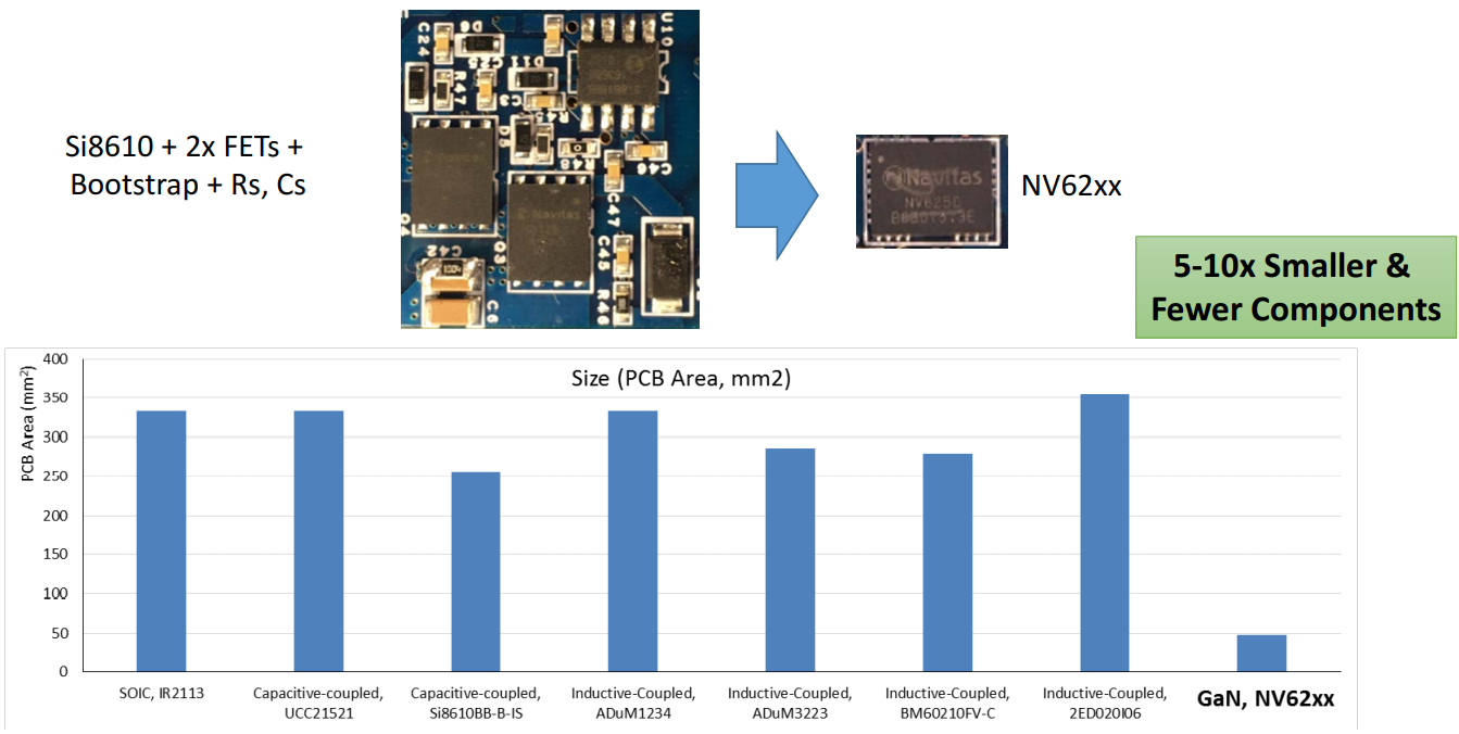
Eliminating Footprints and Complexity
High-Frequency Half-Bridge Integration

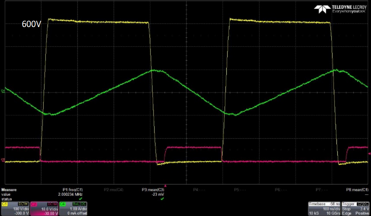
Half-Bridge GaN Power IC at 2 MHz
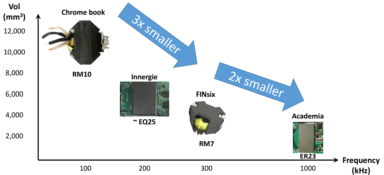
Frequency Drives Transformer Size & Cost (65W)
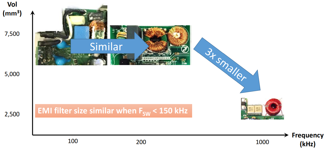
Frequency Drives EMI Filter Size & Cost
Conductive frequency range: 150 kHz – 30 MHz
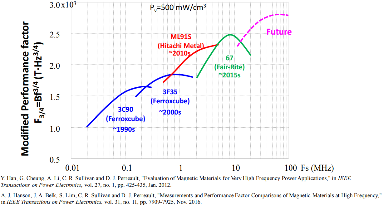
Magnetics’ Frequencies – 10x Every 10 years
GaN Power ICs enable Hi-Density Adapters
3x Higher Density with 50% Energy Savings
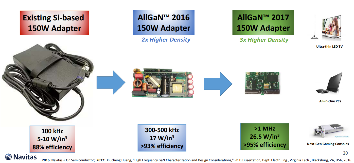
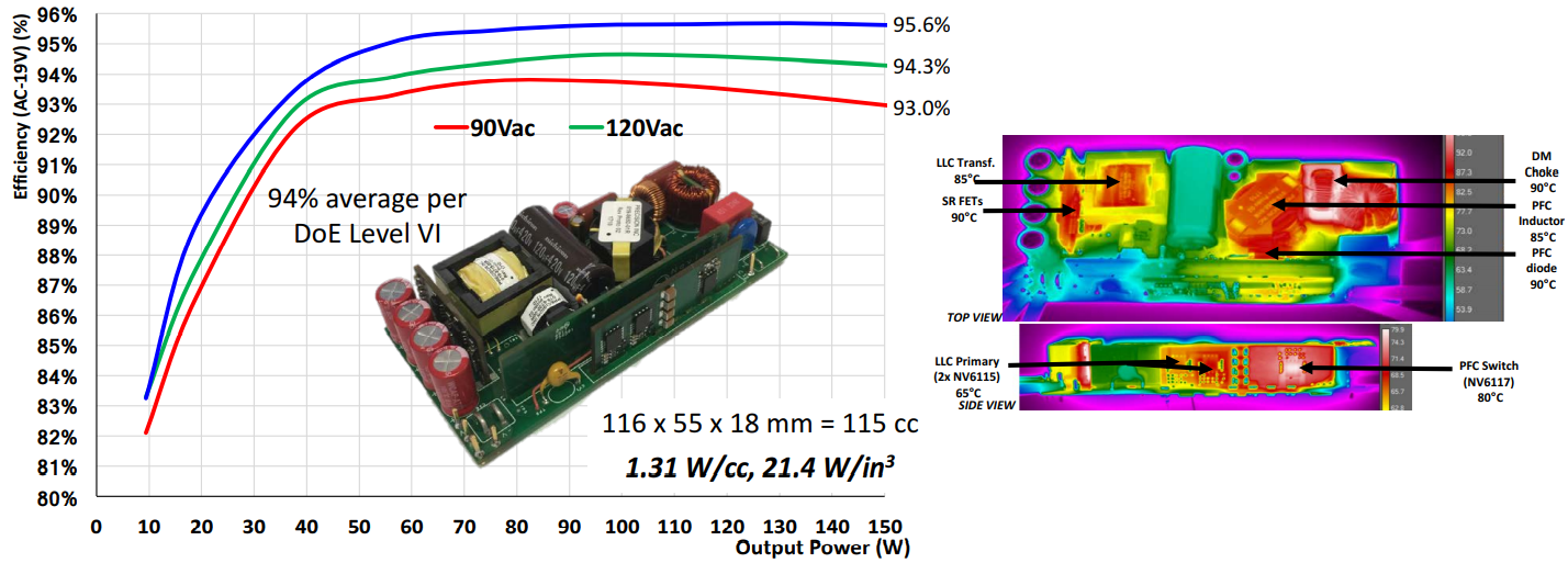
AllGaN: 150W, PFC+LLC, 300 kHz → Over 20W/in3
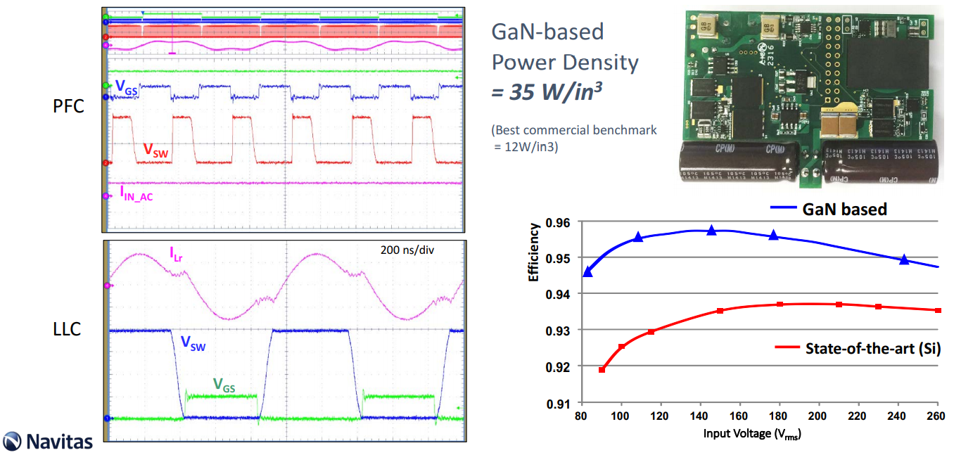
AllGaN: 150W, PFC+LLC, >1Mhz → 35W/in3
Fast Chargers … going “GaN Fast”
3x Fast Charging with 50% Energy Savings
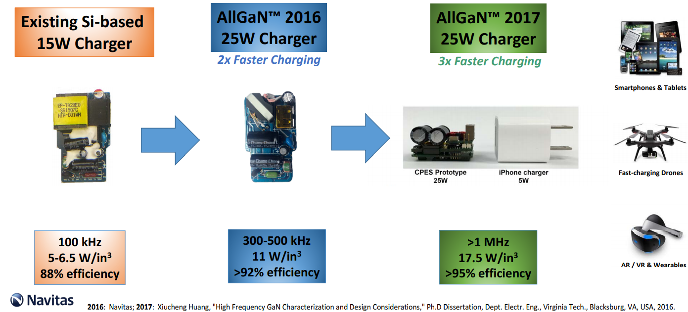
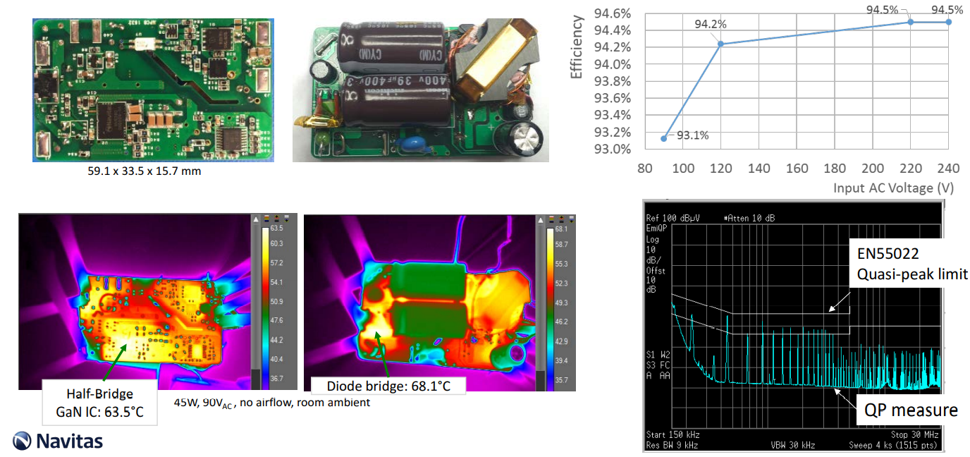
AllGaN: 45W, ACF, 300kHz → 2-3x Faster Charging
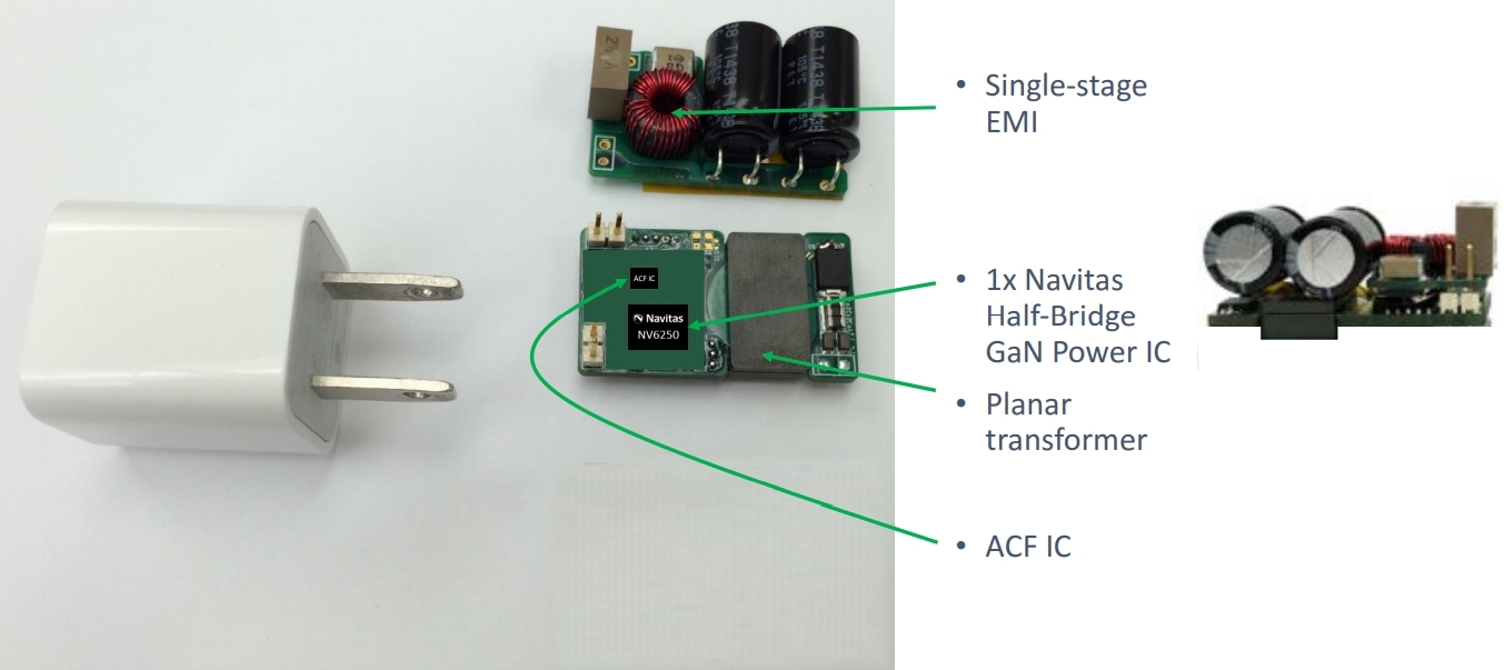
AllGaN: 25W, ACF, >1MHz → 4-5x Faster Charging
Time for Another Disruption…
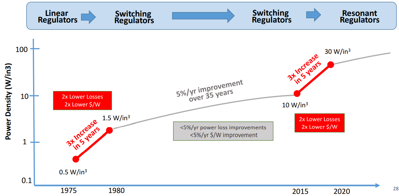
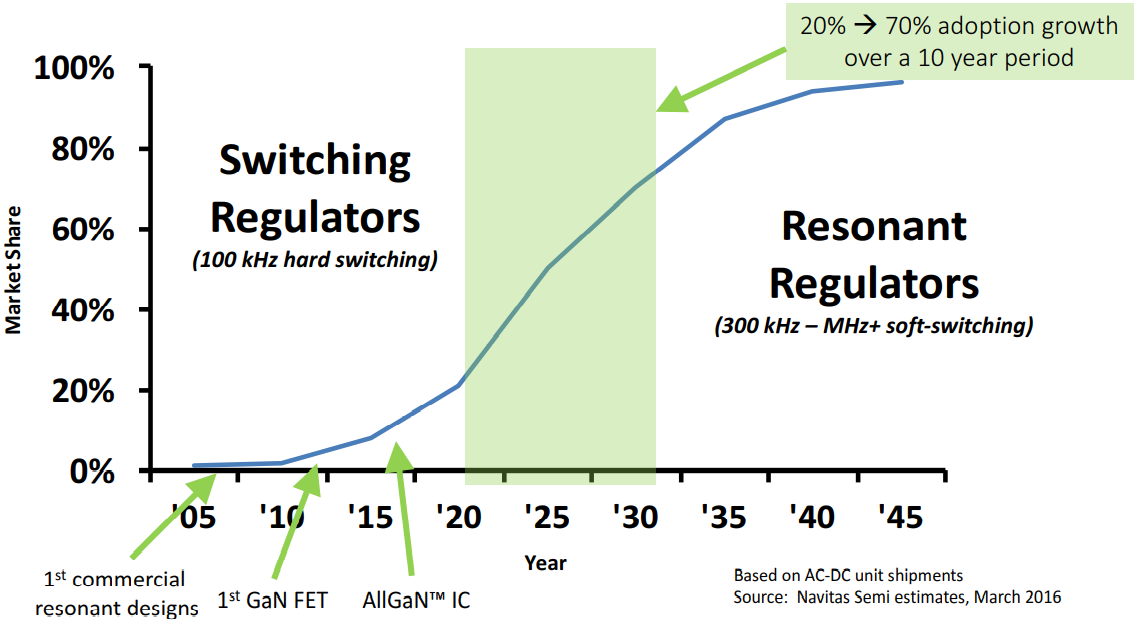
High-Frequency Resonant Market Adoption
