GaNSense™ Half-Bridge Integration Accelerates the Power-Electronics Revolution
![27_Pdf_File_Type_Adobe_logo_logos-512[1]](https://navitassemi.com/wp-content/uploads/2020/12/27_Pdf_File_Type_Adobe_logo_logos-5121.png)
GaNSense™ Half-Bridge Integration Accelerates the Power-Electronics Revolution
By Stephen Oliver, VP Corporate Marketing & Investor Relations
Five years into the second revolution in power semiconductorsi, gallium-nitride-(GaN)-based mobile fast-chargers dominate flagship smartphone and laptop models, taking market share from legacy power silicon chips. This next-generation ‘wide band-gap’ technology is cascading into mainstream mobile applications and simultaneously breaking-out from that beachhead market, into higher-power consumer, solar, data centers and EVsii. A new power-platform – the integrated, feature-rich, high-efficiency GaNSense™ ‘half-bridge’ – is a fundamental building-block in highpower, high-speed applications, where GaN not only delivers smaller, fast-charging and lower system-cost applications, but also can save an estimated 2.6 Gtons of CO2/year by 2050iii.
Fundamental building blocks: full-bridge and half-bridge architectures
One of the simplest methods to measure current is to add a shunt series resistor into the current path of interest, and then measure the voltage across it as a representation of that current, knowing the relationship of Voltage = Current * Resistance, (V = I*R), and assuming a stable, or linear, resistance.

Figure 1: Half-Bridge configuration is a fundamental building block in power electronic circuits
Speed #1: Soft-switching optimizes power-conversion performance
High-speed – or rather, high-switching-frequency – operation shrinks the size, weight and cost of ‘passive’ elements (transformers, capacitors, EMI filters, etc.) within a power system. However, simply running a standard topology at high speed means extreme losses and reliability risks due to silicon’s highly-capacitive material properties. ‘Soft-switching’ is a control technique in which excess voltage and/or current across a power device are eliminated before the device is switched on or off, avoiding capacitive- or switching-speed-related losses. The summary below details the efficiency benefits of soft- vs. hard-switching, and also highlights the material advantage of GaN power ICs vs. legacy Si discrete FETs.iv
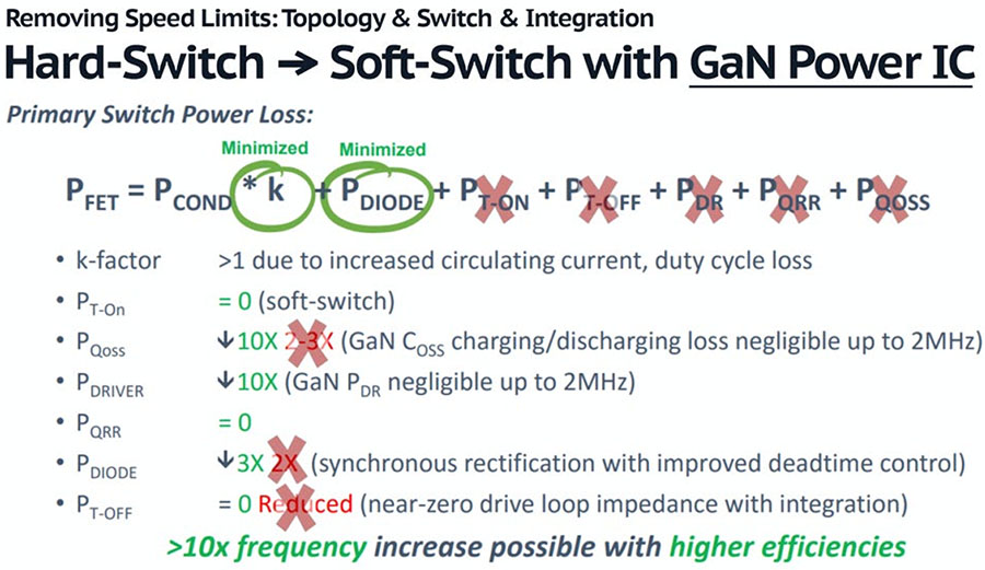
Figure 2: Using GaN Power ICs in soft-switching topologies eliminates turn-on losses, device recovery and driver losses.
Moving up to higher powers, multi-kW AC-DC power supplies for data centers host several softswitching, half-bridge elements. A typical design is split into two sections: the first for mains ACDC rectification and ‘power-factor correction’ (PFC), with the second ‘DC-DC’ stage combining isolation and voltage step-down functions. Modern designs use a ‘totem-pole’ (TP) structure which combines AC-DC and PFC functions by using two half-bridge circuits, one operating at a low speed to handle the AC mains frequency (50-60 Hz) and the other at 100’s of kHz or MHz+ to control the PFC. The DC-DC stage is another half-bridge, typically in an LLC topology, or sometimes full-bridge for higher power, and again running at high switching-speeds. An example 3.2 kW “MHz” design is shown, with variable-frequency boundary-mode T-P PFC running between 500 kHz and 1.5 MHz, and downstream DC-DC running at 1 MHz, delivering impressive power density, 2x higher than typical industry-standard W/ccviii. This is an ‘all-GaN’ powertrain design, with 650 V GaNFast power ICs for the PFC and DC-DC primary, and 200 V GaN FETs for the DC-DC secondary.

Figure 3: 3.2 kW Server Power Supply using GaNFast Power ICs for Totem-Pole PFC and LLC in MHz switching to achieve 98% efficiency and 4.4 W/cc
Speed #2: Motor-drive applications spin the hard-switch exception.
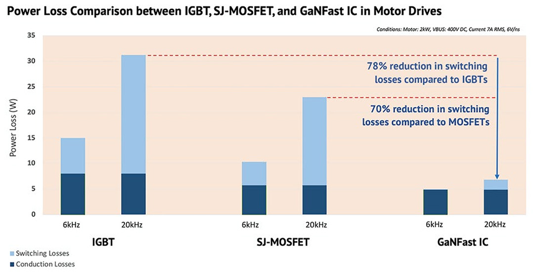
Figure 4: GaN achieves a 78% reduction in total power loss, while simultaneously running 3x faster than a legacy Si IGBT design.
Integration: Introducing the GaNSense™ Half-Bridge
Historically, power designers had to create half-bridge circuits from discrete transistors and a myriad of external controllers, sensors and peripheral components. Now, new, easy-to-use, highperformance GaNSense Half-Bridge power ICs are available in small 6 x 8 mm surface-mount PQFN packages for a broad range of applications from 200 W TV / monitors to 1 kW motor-drives. Highly integrated, these next-generation power ICs combine two GaN power FETs with GaN drive, plus control, sensing, protection and isolation.
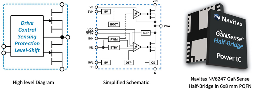
Figure 5: GaNSense half-bridge integrates drive, control, sensing and protection, with level shifting isolation, into a single 6×8 mm PQFN package
Unlike complex, costly and potentially unstable discrete implementations, the GaNSense half bridge includes advanced features to simplify design such as standard digital-logic inputs, high-side bootstrapping and level-shifting, and loss-less current-sensing for the highest efficiency and maximum chance of first time-right, fastest-time-to-market designs. As a true IC, protection features such as overcurrent, over-temperature sensing and autonomous control, shoot-through protection, 2 kV ESD and 200 V/ns slew-rate capabilities come as standard. Compared to discrete GaN solutions, the GaNSense half bridges deliver a 60% reduction in both component count and PCB area, eliminate unreliable operation, deliver 6x faster ‘detect-to-protect’ operation and higher efficiency. The NV6247 (2x 160 mΩ) and NV6245 (2x 275 mΩ) half bridges are the first available with a higher-power portfolio to follow.
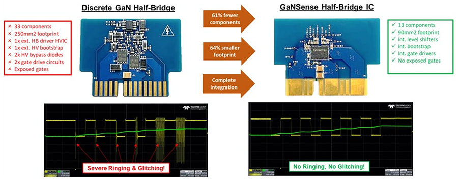
Figure 6: GaNSense half-bridge IC solution offers smallest PCB area, fewest components, with no ringing and no glitching during switching transitions
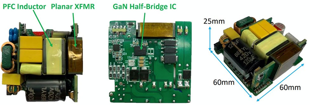
Figure 7: 140W fast charger using GanSense half-bridge IC in asynchronous half-bridge (AHB) topology to achieve 93.5% efficiency at 1.1 W/cc.
Standard motor drives have a lossy current-sensing resistor in each of the lower-legs of the threephase topology. This sense resistor is a burden to the designer in terms of energy loss, PCB space, component count, cost and reliability due to higher temperatures. With GaNSense, these three points of loss are immediately eradicated, leading to lower temperatures, more energy savings and smaller, more reliable systems. For higher-power systems, arrays of single GaNFast power ICs with high-speed digital-isolators create kW+ half-bridge building-blocks that enable EV OBCs, traction drive, large-scale air-conditioning, heat-pumps, etc.

Figure 8: Integrating a complete half-bridge stage with loss-less phase-current sensing and autonomous short-circuit protection allows simplest and most compact solution.
Market expansion, and acceleration:
References
i) “From Science Fiction to Industry Fact: GaN Power ICs Enable the New Revolution in Power Electronics”, Oliver, Xu & Huang, article in Bodo’s Power magazine, May 2017.
ii) “Introduction to Wide Band-Gap Semiconductors”, Navitas website.
iii) “Electrify Our World™”, Navitas 2021 Sustainability Report and CarbonNeutral® certification.
iv) “Breaking Speed Limits with GaN Power ICs”, Kinzer, keynote at APEC, March 2016.
v) “GaN ICs Enabling Next-Gen ACF for Adapter/Charger Application”, Huang, industrial paper, APEC, March 2019.
vi) “Here come the GaN Chargers”, Oliver, conference presentation, Bodo’s Power Conference, December 2019.
vii) “Navitas Powers World’s Fastest Smartphone Charging Technology from realme at MWC 2022”, Navitas press release, March 2022.
viii) “High-frequency and high-density design of all GaN power supply unit”, Yu et al., UT Austin, IEEE conference paper, PCIM 2018.
ix) “Integrated Motor Drive using Soft-Switching Current-Source Inverters with SiC- and GaN-based Bidirectional Switches”, Dai et al., conference paper, 2020 IEEE Energy Conversion Congress and Exposition (ECCE).
x) “Motor drive based on III-Nitride Devices”, Battello, Oliver, US patent 8,390,241 B2 Mar. 5, 2013.
xi) “Autonomous GaN Power ICs Deliver High-Performance, Reliable Motor Drives”, Hesener, article, Power Electronics News, May 2022.
xii) “GaN Half-Bridge ICs Enable Next Gen Mid-Power, Multi-Port, High-Density Charger Topologies”, Ribarich, industrial paper, APEC, March 2022.
xiii) “Navitas Celebrates 50,000,000th GaN Shipment with vivo”, Navitas press release, May 2022.
xiv) “Navitas Announces World’s First 20-Year Warranty for GaN ICs”, Navitas press release, March 2022.