Powering AI: Efficient, Scalable, Sustainable with GaN and SiC
The adoption of generative AI has brought step-change benefits to many industries and its use has increased exponentially in recent years. Development is being led by many of the world’s largest technology companies such as OpenAI, Microsoft, Google and Amazon Web Services.
With exponential growth in use comes exponential growth in power consumption, and this is putting the net-zero targets of these companies, and the countries in which they operate, at risk.
Amazon is already the world’s largest corporate purchaser of renewable energy. Google has signed up to the largest renewable energy deal in history. Microsoft is looking to develop their own nuclear power plants to supply clean energy for its AI data centers. But many believe this is not enough.
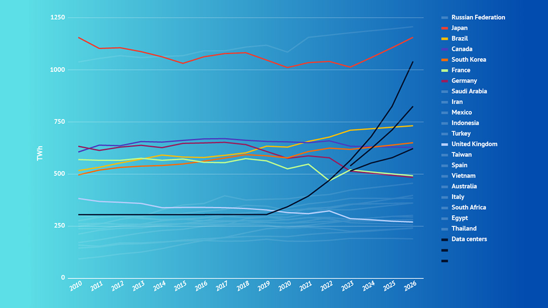
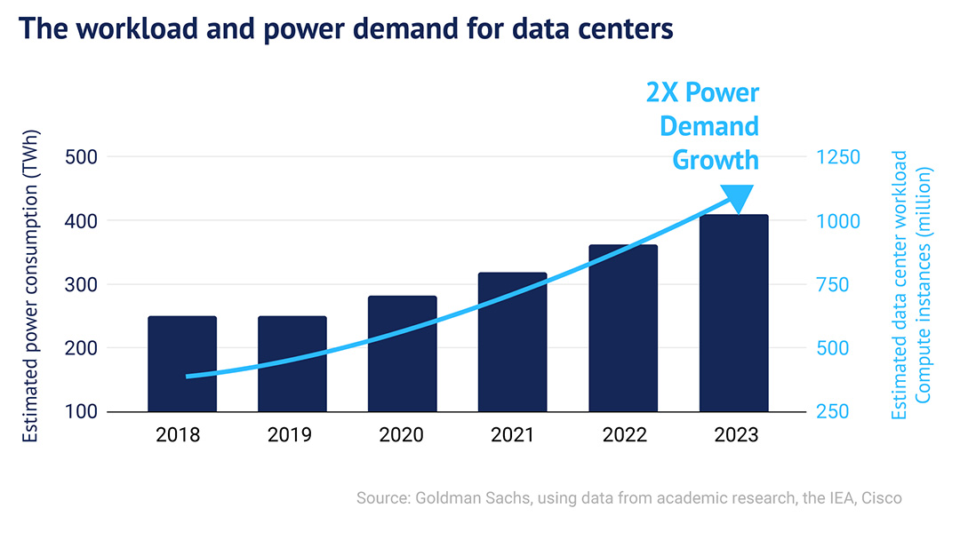
The International Energy Agency has forecast that combined global data center electricity consumption will reach 1,000 TWh by 2026. Yet, planning regulations in many western countries have limited the building of additional renewable energy capacity, with AI power consumption accelerating faster than renewable energy capacity globally.
Bloomberg analysis has suggested AI will consume more energy than all but 12 countries by 2030.
Energy efficiencies are therefore being looked at across the system, with the processors, cooling, and power supply inefficiencies (respectively) being the three largest uses of this power.
Standards for power supply efficiency exist, notably 80 PLUS. The standard is voluntary; however, the efficiency ratings outlined in the 80 PLUS Titanium standard have been adopted by the European Union for its EcoDesign standard, which is mandated for use by AI data centers operating in the EU. The Titanium-level certification stipulates efficiencies of 96% in PSUs.
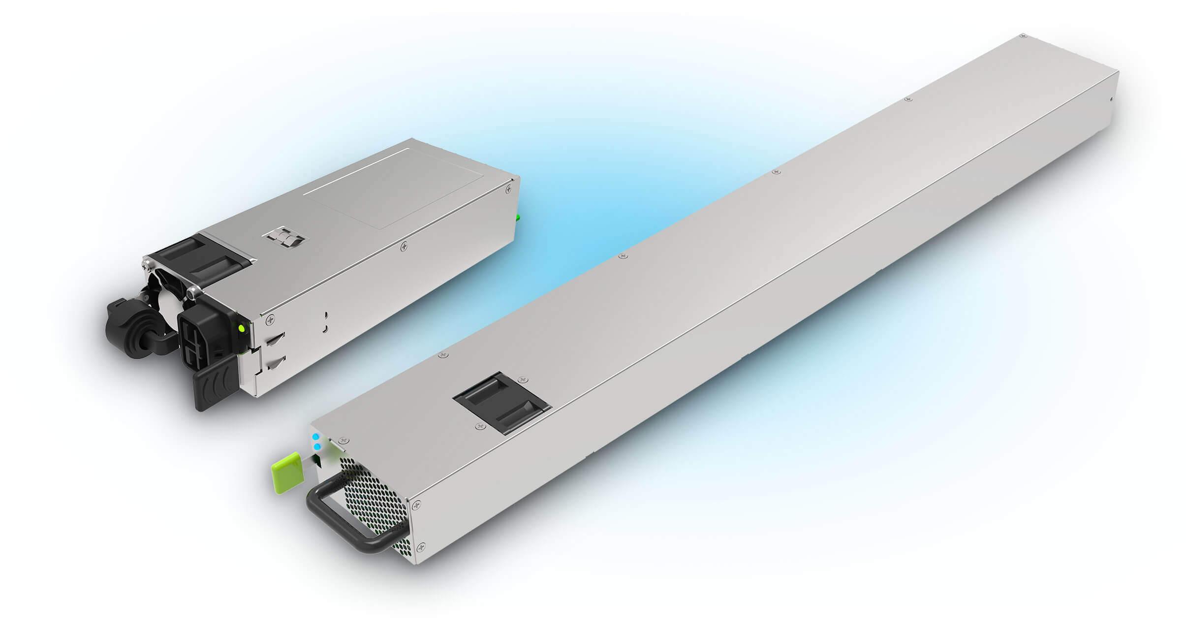
With power supplies units (PSUs) for AI data centers using standard (CRPS or OCP) form factors, these increases in energy consumption necessitate an increase in power densities too.
Until recently silicon was the main material used in semiconductors for power supplies, but the performance and efficiency requirements of next-generation PSUs for AI applications are exceeding silicon’s limits. As a result,the industry is turning to wide bandgap materials, such as silicon carbide (SiC) and gallium nitride (GaN) to meet processing demands as effectively as possible.
Energy Consumption in AI Data Centers
Current Energy Usage
As a result of the growth in AI, energy consumption by data centers is rising rapidly. Data from the International Energy Agency (IEA) suggests that in 2022 alone, approximately 460 terawatt-hours (TWh) were consumed globally by data centers[1], approximately 2% of global energy production. In the US, data centers accounted for approximately 3% of all energy consumed[2] in 2023.
Indeed, the rise in energy consumption in data centers is placing the net-zero ambitions of companies[3] and countries[4] at risk and some regions/countries are placing tighter planning restrictions on new developments[5]. As such companies are investigating alternative energy sources, including renewables investment and the construction of small-scale nuclear facilities to power their AI[6].
While AI adoption is still small, power consumption by data centers is set to grow significantly, and annual power efficiency gains have slowed from ~18% (2016) to ~1% (2023)[7].
Growth Trends
It is widely predicted energy consumption will grow significantly. The IEA has stated that electricity consumption from data centers could reach more than 1,000 TWh by 2026. And the US alone will reach this figure just four years later[2], with Goldman Sachs suggesting the share of power used by data centers will more than triple over the course of this decade (2020 – 2030), to c.8% [2] and attributing virtually all of the acceleration in electricity demand to AI.
Sweden is expected to see energy use from data centers double as a result of AI by 2030, and double again by 2040[8]. In the UK, AI energy use is set to rise more than 5X over the next 10 years[8].
Bloomberg estimates that there are more than 7,000 data centers that are either built or in construction, This compares with 3,600 in 2015[8]. And their energy consumption by 2034 will be approximately the same as the entirety of India[8].
This growth in energy consumption for AI data centers is also being driven by a consumer shift towards using generative AI as a search engine, with ChatGPT queries being between 6X and 10X as power intensive as traditional Google searches[2].
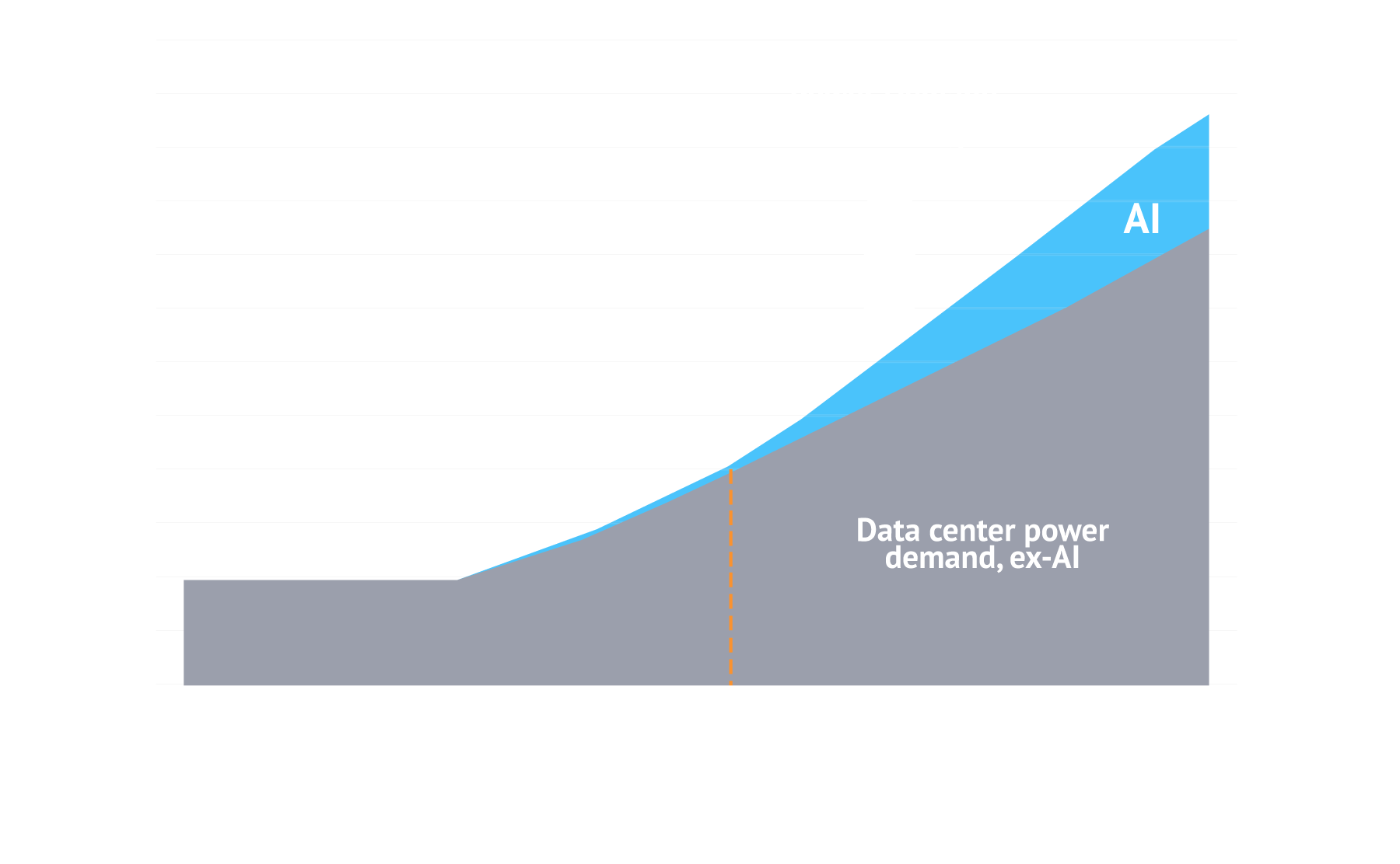
Fig 1 – Based on information from Goldman Sachs
Data centers either built or in construction (as of 2024)
Energy use increase over the next 10 years
Power consumption of ChatGPT query versus Google
Comparison to Other Sectors
Forecasts of US energy demand predict a 2.4% CAGR between 2022 and 2030[8]. According to a report by Goldman Sachs, the growth in energy consumption by AI data centers will be the highest of any of its tracked sectors, contributing 0.9 of these CAGR percentage points (38% of total growth), which is 50% more than the next two biggest causes of increased energy usage: residential (0.6 points) and transportation (0.6 points)[2].
Evolution of AI Chips and Their Power Usage
Early AI Chip Evolution – Pre 2015
In the first years of AI, processing was performed on standard GPUs, rather than specialized hardware.
Core examples include:
- AMD’s FirePro S9150 (launched 2014) was billed as the “most powerful server GPU for HPC” at its launch. This provided 5.07 teraflops with a power consumption of 235 watts[9].
- NVIDIA’s CUDA-enabled Tesla K80 (launched 2014), which was used for deep learning and was able to deliver 8.73 teraflops and consumed 300 watts[10].
AI Evolution – 2015-2019
This period became foundational in advancing machine learning and AI applications, with processors being specifically developed for AI. Examples include:
- NVIDIA’s Tesla v100 (launched 2017) offered 125 teraflops of performance while consuming 300 watts of power[11].
- Google’s Tensor Processing Unit v3 (launched 2018) delivered up to 420 teraflops but consumed c.450 watts[13].
- Intel’s Nervana NNP (launched 2019) is a neural network processor that was created following Nervana’s acquisition in 2016 for $400 million[13]. It delivered 119 teraflops, and implemented a thermal design to reduce power consumption to c.200 watts[13].
AI Evolution – 2020-today
The acceleration in capabilities have increased dramatically, for example:
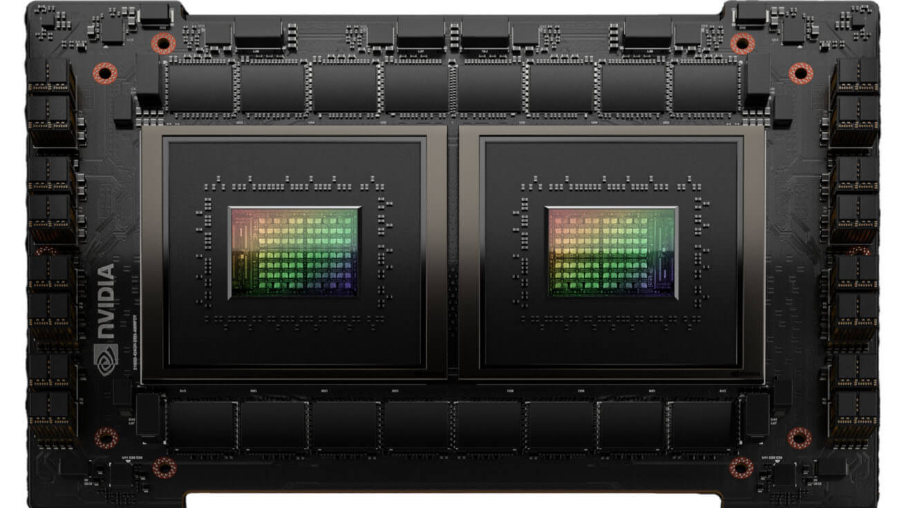
NVIDIA, however, is arguably the best known AI processor manufacturer, with the chipmaker’s share price doubling in the first half of 2024 to make it the world’s most valuable company – as of June 2024[16], and recent evolutions of its server system specifications are indicative of increasing max power per server but with lower power intensity per petaflops.
Operating at 0.32 kW per petaflops, NVIDIA’s DGX H100 (Grace Hopper) is capable of 7X computing speeds but only uses 1.5X the power of NVIDIA’s previous generation (DGX A100)[2]. Specifications for the newly announced NVIDIA Rubin haven’t yet been announced, but its Blackwell DGX B200 server system will improve further on Grace Hopper to enable 72 petaflops, but do so at just 0.2 kW per petaflops. However, this is still a power increase per server system of 40%, shifting from 700 W each for Grace Hopper, to 1,000 W for Blackwell[17] and this necessitates advances in power supplies.
Power Supplies for AI Data Centers
CRPS Power Supply (PSU) Form Factor for AI, Hyperscaler and Data Center Applications
AI and hyperscaler data center power supplies come in three form-factors, CRPS185 (common redundant power supply), CRPS265 and OCP (Open Compute Project). These measure the same width and height (73.5 mm x 40 mm), but vary in length (CRPS185 = 185 mm, CRPS265 = 265 mm, OCP = 600 mm), with these specifications developed and defined by the hyperscale Open Compute Project, whose members include Dell, Facebook/Meta, Google, Intel and Microsoft. By having these common standards, the industry is able to maximize interoperability and therefore simplify upgrades / minimize downtime in the event of a failure[18].
Each unit measures 40 x 73.5 x 185 mm (544 cc). The Increased power demands of AI servers, therefore, necessitate an increasing power density. In addition to increasing power densities, the roadmap for the CRPS form factor also emphasizes improved efficiency, reliability, and manageability.

Fig 3 – Circuit diagram for a CRPS form-factor PSU

Fig 3 – Circuit diagram for a CRPS form-factor PSU
Increasing CRPS Power Densities for AI Data Centers
Multiple challenges exist in increasing power densities, with higher-density power supplies requiring increased thermal management, including heat dissipation, which adds cost and increases energy consumption.
As densities increase, so to do conversion efficiencies, and with this comes a reduced need for thermal management. These increases can be achieved through higher switching frequencies[19], but a fundamental issue in doing so is that silicon has reached its performance limits[20]. In high-density CRPS applications, swapping out silicon MOSFETs with GaN devices allows much higher switching frequencies and supports the use of planar transformers[19].
However, discrete GaN FETs have relatively fragile gates, and solutions in which they are used can experience problematic high-side and low-side ringing and shoot-through currents. This issue has been solved by monolithically-integrating a GaN gate driver circuit on the same chip as the GaN FET[19].
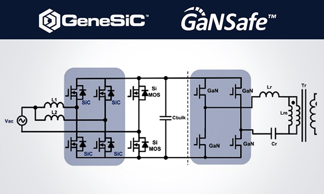
Fig 4 – Circuit diagram for next-generation CRPS form-factor PSU using GeneSiC and GaNSafe power ICs to increase power density for AI applications
Power Supply Standards and Compliance
To minimize the power consumed through losses in the power supply, industry standards have been applied. The key standard for the PSU sector is the 80 PLUS certification[21].
80 PLUS Certification
80 PLUS certification is a voluntary program for PSU manufacturers and is aimed at encouraging manufacturers to produce more energy efficient products[21].
At its base level, it specifies that PSUs are a minimum 80% efficient at 20%, 50% and 100% of load with a 230 V input. Since its inception in 2004, five additional levels of increasing efficiency have been added to further improve PSU efficiency as technologies develop. For 230 V Internal supplies, these range from the Bronze (81% at 20% load, 85% at 50% load and 81% at 100% load), Silver (85%, 89% and 85% at these loads), Gold (88%, 92% and 88%), Platinum (90%, 94% and 91%), with 230 V EU internal supplies typically having increased efficiency requirements for each of the 80 PLUS levels. Since 2012, the top standard has been Titanium.[21].
80 PLUS Titanium
The 80 PLUS Titanium standard requires that PSUs are 90% efficient at 10% of load, 96% at 50% and 91% at 100% of load with a 230 V input[21].
While not officially mandating the standard, the EU has aligned its EcoDesign Directives with the 80 PLUS certification standard and data centers, including those for AI, operating in EU territories are legally required to comply with these EcoDesign Directives[22].
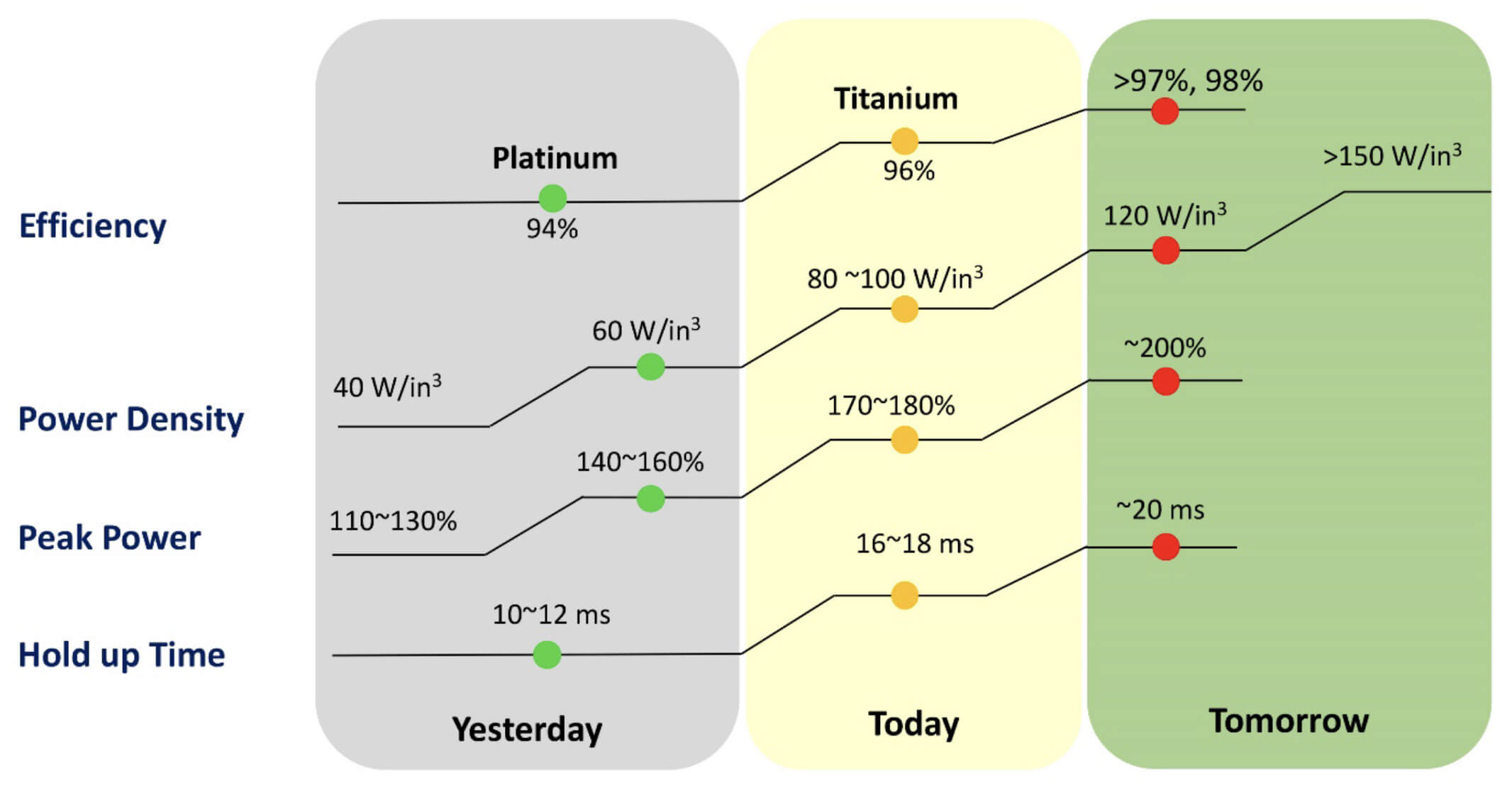
Fig 5 – The 80 PLUS PSU efficiency standard is set to become ever more stringent
Beyond Titanium
It is widely expected that future PSUs for AI data centers will be required to comply with a next-generation 80 PLUS certification standard[19].
For this we can expect required efficiencies of over 97% efficiency at 50% of load, as well as increased power densities, peak power and hold up time[19].
Materials for PSUs – Silicon vs. Wide Bandgap Materials
Silicon
The most-commonly-used topology for data center server power supplies employs silicon MOSFETs and has a boost power factor correction (PFC) stage followed by an LLC resonant converter. Increasing power demands associated with AI workloads requires multiple outputs when using LLC transformers to minimize conduction losses of secondary windings and synchronous rectifiers (SRs). Combining windings and SRs in parallel can achieve lower winding resistance but the more pronounced termination losses this causes (as switching frequency increases) negatively impacts overall system efficiency[22].
Due to the limitation on the number of PCB windings possible within the circuit board structure, they can only be used when the switching frequency is high enough to support a minimum number of turns. This means silicon is at its performance limits for PSUs and will not be able to improve efficiency to meet the needs of AI[22].
Wide Bandgap Semiconductors in PSUs
Bandgap is the energy needed to free an electron from its orbit around the nucleus. As this directly determines the withstandable electric field for a given material, a wider bandgap enables the development of semiconductors with very short or narrow depletion regions[23].
This enables device structures that possess very high carrier densities, and therefore smaller transistors and shorter current paths with ultra-low resistance and capacitance, as well as switching speeds that are orders of magnitude higher[23].
Bandgap is measured in eV (electron volts) [23], with Silicon having a bandgap of 1.12 eV[24].
Silicon Carbide
Silicon carbide (SiC) is a compound known for its exceptional properties, such as high thermal conductivity, high electric field breakdown strength, and excellent thermal stability. It has a bandgap of 2.26 eV[23]. SiC-based components can operate at higher temperatures and voltages than their silicon counterparts, resulting in more efficient power conversion and reduced energy losses.
SiC MOSFETs and diodes enable faster switching speeds and lower power losses[25], enhancing the overall efficiency and while their physical and switching properties tend to make them more applicable to automotive, industrial, and renewable energy sectors[25], CRPS PSU reference designs created by Navitas have incorporated the GeneSiC™ power IC, alongside a gallium-nitride (GaN) power IC, to enable increases in power density and efficiency[19].
Gallium Nitride
With a bandgap of 3.39 eV[23], GaN possesses a high electron mobility and these devices allow much higher switching frequencies and support the use of planar transformers[19].
As noted, discrete GaN FETs have relatively fragile gates, which for PSUs necessitates the use of a monolithically-integrated GaN gate driver circuitry on the same chip as the GaN FET in order to prevent high-side and low-side ringing and shoot-through currents[19].
For example, Navitas’ GaNSafe™ has high-speed protection with autonomous ‘detect and protect’ that acts within 50 ns. ESD protection is also implemented to protect against events up to 2 kV. And to protect against extraordinary application conditions, GaNSafe integrates a 650 V continuous and 800 V transient voltage rating[19].
Efficiency of Wide Bandgap PSUs
Power ICs using GaN and SiC have already been implemented for CRPS-form factor PSUs. This includes Navitas’s 3.2 kW CRPS platform[18].
In addition, a 2024 reference design for an AI data center server PSU has been created using Navitas’ GaNSafe and GeneSiC families of products[19]. The reference design for a 54 V AC-DC data center AI server power supply uses a CRPS185 form factor. Data from the design showed an increased efficiency of >97% with an increase in power density from 98W/in3 to 137W/in3 versus a comparable 3.2 kW CRPS solution – translating to a power output of 4.5 kW. The test data from this reference design also showed it was possible to reduce waste power and mitigate the need for additional thermal management provision[19].

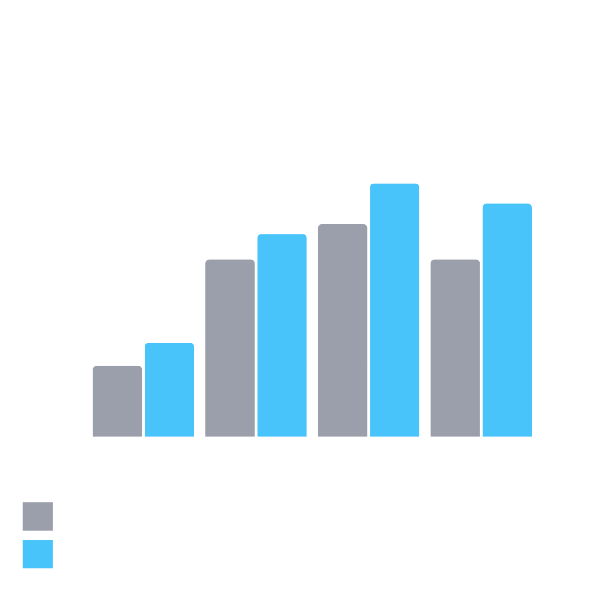

Fig 6 – 54 V AI/GPU server reference design performance improvements in comparison to existing 3,200 W CRPS solution
App Notes, Articles
World’s First 12 kW PSU for Hyper-Scale AI Data Centers using GaN and SiC
Read More
Achieving Next Generation Power Density and Efficiency for AI and Hyperscale Data Center PSUs
Read More
World’s First 8.5 kW PSU for AI Data Centers using only GaN and SiC
Read More
High-Density Power for the AI Revolution
Read More
AI Tech Features
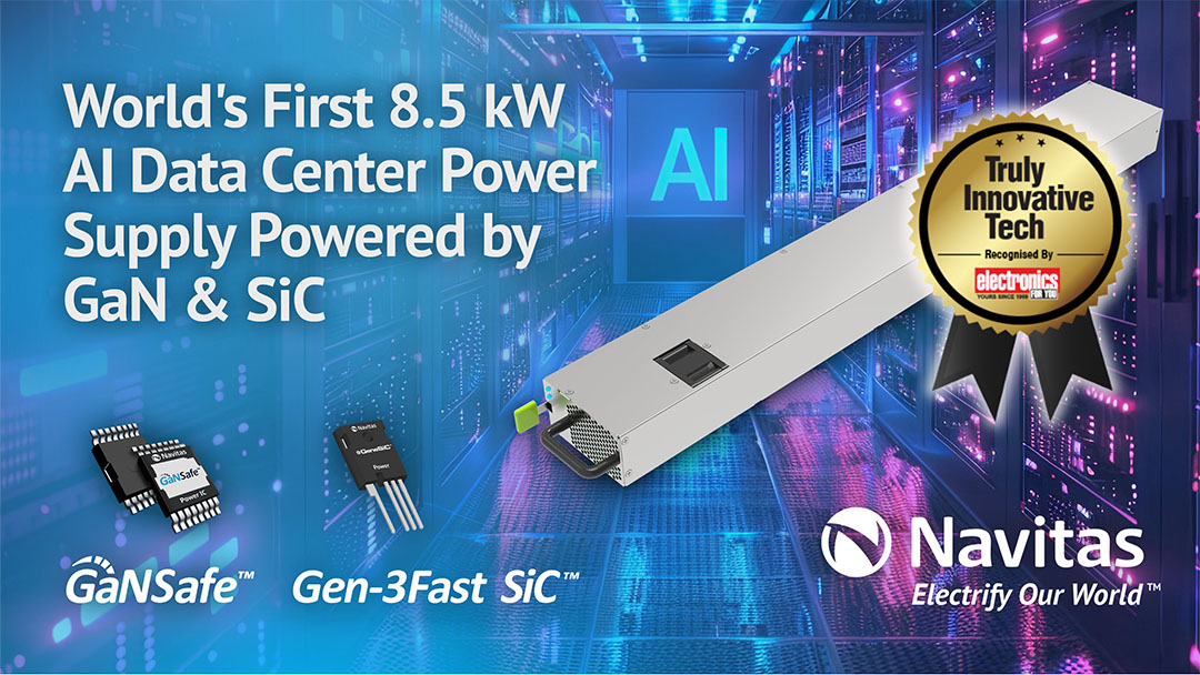
Navitas 8.5kW PSU Designed for AI Data Centers Wins Electronics For You Innovation Award
Navitas Semiconductor's 8.5kW power supply unit (PSU), powered by GaNFast™ and GeneSiC™ technologies, has been recognized for its innovative design. Tailored for AI and hyperscale data centers, the PSU achieves 98% efficiency while meeting Open Compute Project...
Data Centers Burned More Power in 2022 Than 185 of the World’s 195 Countries.
And this is forecast to rise to 190 by 2026 Fig 1: Data centers global share of energy consumption will grow from being the 11th biggest electricity consumer in 2022 to the 6th biggest in 2026.* Data Center Consumption According to 2024 data from the International...
Nvidia’s Grace Hopper Runs at 700 W, Blackwell Will Be 1 KW. How Is the Power Supply Industry Enabling Data Centers to Run These Advanced AI Processors?
Blackwell configurations will require 60 kW to 120 kW per rack but fewer than 5% of the world’s data centers are capable of supporting even 50kW per rack Generative AI’s proliferation is far from complete, but its rise has been (without trying to hyperbolise) little...

