Accelerating to NetZero
“The Navitas mission is to ‘Electrify Our World™’ with next-generation power electronics that will accelerate our transition to a sustainable, clean energy economy.”

Chris Allexandre, President & CEO
Navitas: World’s First CarbonNeutral®-Certified Semiconductor Company
In May 2022, Navitas Semiconductor announced that it was the world’s first semiconductor company to achieve CarbonNeutral®-company certification from the leading experts on carbon-neutrality and climate finance, Climate Impact Partners. Certification has continued, now including the GeneSiC team and portfolio.
Achieving CarbonNeutral-company certification is another milestone towards Navitas’ mission to “Electrify Our World” and to help Navitas’ customers achieve their own sustainability goals.
Sustainability Report 2022
The transition from silicon chips to gallium nitride (GaN) and silicon carbide (SiC) will play a vital role in enabling and accelerating a variety of industries to achieve the goal of net zero carbon emissions by 2050.
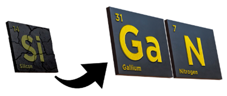
Navitas creates next-generation power semiconductors using GaN and SiC, replacing legacy silicon chips in power conversion and battery-charging applications.
GaN power ICs are efficient, cost-effective and enable up to 3x more power and 3x faster charging in half the size and weight of old silicon solutions. Gallium metal is a non-toxic, non-conflict, readily available byproduct from aluminum smelting.
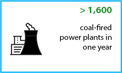
The CO2 footprint to manufacture and ship GaN is up to 10x lower than silicon and reduces end application footprint by up to 30%. Improvements in the performance of electric vehicles (EVs) could accelerate worldwide EV adoption by three years and save up to 20% of road-sector emissions by 2050. Each GaN power IC shipped saves net 4 kg CO2, and GaN offers the potential to address a reduction of 2.6 Gtons CO2 /year by 2050 – equivalent to the CO2 generated by over 650 coal-fired power stations, over six billion barrels of oil, over 560 million ICE passenger cars – or the annual electricity use of over 470 million homes. 1 2
SiC power semiconductors are optimized for higher-voltage, higher-power applications, such as solar, EV, long-haul trucking, railway locomotives, grid-tied applications, etc.
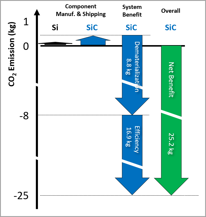
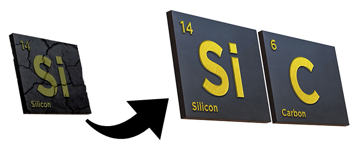
While a SiC FET requires more energy to create than a Si IGBT – due to SiC boule growth – the system benefits in terms of dematerialization and efficiency upgrades for higher-power, longer-lifetime systems, far outweigh the initial footprint. In fact, each SiC FET shipped is estimated to save 25.2 kg of CO2 vs legacy silicon IGBTs. SiC offers the potential to address a further reduction of 3.4 Gtons CO2 /year by 2050.
What is GaN?
What is SiC?
How do they “Electrify Our World™”?
Combining gallium and nitrogen, gallium nitride (GaN) is a ‘wide bandgap’ semiconductor material with a hard, hexagonal crystal structure with a 10x stronger electric field and 2x higher electron mobility than silicon. Gallium does not exist in elemental form in nature but is a by-product from the smelting of bauxite ore into aluminum, so is readily available, low cost and has a very low extraction and refinement carbon footprint – and nitrogen is in the air we breathe.
![ganfast-and-sic[1]](https://navitassemi.com/wp-content/uploads/2023/12/ganfast-and-sic1.jpg)
GaN enables up to 3x more power or 3x faster charging, with up to 40% energy savings in half the size and weight of legacy silicon. Navitas’ GaNFast power ICs integrate GaN power and drive plus protection and control to deliver the simplest, smallest, fastest and highest performance.
With its higher thermal-conductivity and lower-frequency operation, SiC is more suited for higher-power applications including the higher-end voltages required in EVs and data centers, some solar-power designs, rail traction, wind turbines, grid distribution and industrial and medical imaging that need higher-voltage operation and improved heat dissipation.
The International Energy Authority (IEA) has defined an ‘ambition gap’ between nations’ public commitments and the target required for us all to meet the maximum 1.5°C rise in global temperatures per the Paris Accord.3
GaN and SiC are critical enablers to address the ‘ambition gap’ as we transition from majority fossil fuel to majority renewable, electricity-based energy sources and uses.
“GaN and SiC accelerate the transition from fossil fuels to renewable energy sources and electricity-based applications”
GaN and SiC make electrical energy more efficient and lower cost, all of which will serve to accelerate the world’s move from coal-fired power plants to solar- and wind-based energy sources and to evolve energy applications from gas-powered transportation, buildings and industrial factories to clean, electricity-based energy.
Progressive Partnerships
Navitas is part of a world-wide eco-system dedicated to sustainability.
References, memberships, commitments, auditors and partners include:

Greenhouse Gas (GHG) Protocol – establishes comprehensive global standardized frameworks to measure and manage greenhouse gas (GHG) emissions from private and public sector operations, value chains and mitigation actions. Protocol defines Scope 1, 2 and 3 emissions on a corporate basis. Navitas corporate reporting uses GHG Protocol standards.
![1024px-DNV_GL_logo.svg[1]](https://navitassemi.com/wp-content/uploads/2023/11/1024px-DNV_GL_logo.svg1_.png)
Det Norske Veritas (DNV) – respected, independent expert in assurance and risk management, including collaborations to assess and forecast benefits of next-generation GaN power ICs across worldwide, multi-market opportunities.

Navitas supports the UN Framework Convention on Climate Change’s (UNFCCC) Sustainable Development Goals (SDGs). The Paris Agreement is a legally binding affordable energy, industry innovation and international treaty on climate change, infrastructure, and climate action.

Capital Impact Partners (CIP) – third-party advisors on sustainability, CarbonNeutral® certifiers.

Science-Based Targets Initiative (SBTi) – in July 2021, Navitas committed to the Business Ambition for a maximum 1.5°C rise in global temperatures by the 2050 deadline set by the 2015 Paris Accord.

The Paris Agreement is a legally binding international treaty on climate change, adopted by 196 Parties at COP 21 in Paris, on 12 December 2015 and entered into force on 4 November 2016. Its goal is to limit global warming to well below 2, preferably to 1.5°C, compared to pre-industrial levels.

Earth-Shift Global (ESG) – respected, third-party organization for independent life-cycle assessments (LCA, estimate of CO2 footprint from product design to disposal / recycling), for assessments of GaNFast power ICs and 65 W mobile charger LCA baselines, per ISO14040/14044. Also partnered with Navitas for initial investigation into GeneSiC SiC component manufacturing carbon footprint, and use-phase assessment of EV on-board charger application.

TSMC– world-class wafer manufacturing partner, with clear commitments to sustainability. Partner for Navitas GaNFast manufacturing.
Aggressive Reduction in Corporate Emissions
CO2 emissions are grouped into ‘scope’ categories per the Greenhouse Gas (GHG) Protocol. As Navitas operates a ‘fabless’ manufacturing model, partnering with world-class companies such as TSMC and X-FAB for wafer/chip manufacturing, and with no company-owned facilities or vehicles, Scope 1 (direct) CO2 emissions are zero.
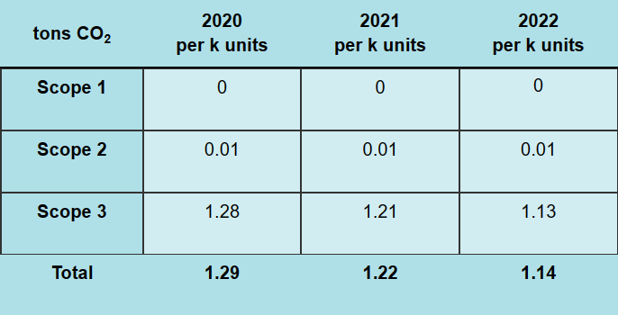
Scope 2 (energy purchases) and Scope 3 (up-stream activities, waste, etc.) are shown below.
On a per-unit basis, emissions were reduced in 2021 by 5%, with a goal to reduce emissions in 2022 by an additional 3% or more. The 2022 result beat the targets, with a 6% reduction on a per-unit basis.
Navitas uses a comprehensive life-cycle assessment (LCA) approach to determine CO2 footprint and report based on GHG protocols.
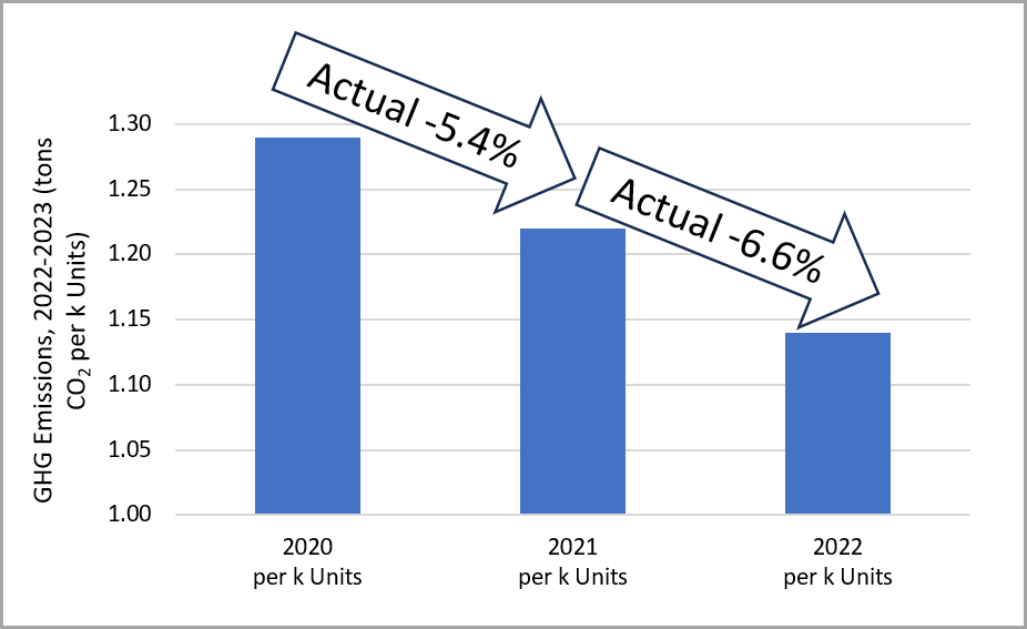
Corporate per-unit CO2 footprint 2020-2022, for GaN
Navitas Semiconductor GHG Emissions Summary, 2020-2022 GaN-Only Data

Navitas Semiconductor GHG Emissions Summary, 2020-2022 GaN-Only Data

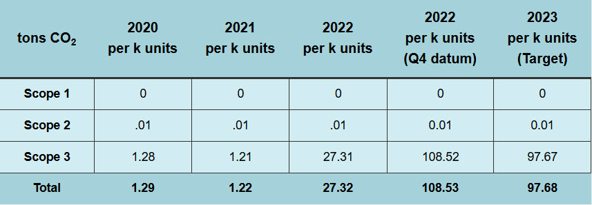
The 2021 data are GaN only. In August 2022, Navitas acquired GeneSiC Semiconductor with leading-edge silicon carbide (SiC) MOSFETs and diodes. For corporate emissions, Q4 2022 is used as a new baseline for the combined GaN and SiC output. On a run-rate (per k unit) basis, the corporate target for 2023 is a 10% reduction in per-unit CO2 footprint vs. the Q4 2022 baseline.

Corporate per- k units CO2 footprint 2022 actual (Q4 2022 datum) to 2023 target
Navitas Semiconductor GHG Emissions Summary, 2020-2023 (GaN & SiC)
(*Revised September 2024 with corrected calculations)
| tons CO2 | 2020 Corporate | 2021 Corporate | 2022 Corporate | tons CO2 | 2020 per k units | 2021 per k units | 2022 per k units | 2022 per k units (Q4 datum) | 2023 per k units (Target) |
|---|---|---|---|---|---|---|---|---|---|
| Scope 1 | 0 | 0 | 0 | Scope 1 | 0 | 0 | 0 | 0 | 0 |
| Scope 2 | 143 | 336 | 236 | Scope 2 | .01 | .01 | .01 | 0.01 | 0.01 |
| Scope 3 | 14,315 | 28,871 | 938,855 | Scope 3 | 1.28 | 1.21 | 27.31 | 108.52 | 97.67 |
| Total | 14,458 | 29,871 | 939,091 | Total | 1.29 | 1.22 | 27.32 | 108.53 | 97.68 |
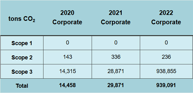
Corporate GHG Emissions by Scope Detail
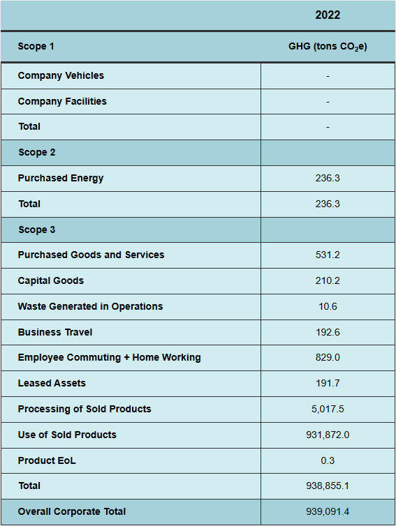
Corporate GHG Emissions by Scope Detail
| | 2022 |
|---|---|
| Scope 1 | GHG (tons CO2e) |
| Company Vehicles | - |
| Company Facilities | - |
| Total | - |
| Scope 2 | |
| Purchased Energy | 236.3 |
| Total | 236.3 |
| Scope 3 | |
| Purchased Goods and Services | 531.2 |
| Capital Goods | 210.2 |
| Waste Generated in Operations | 10.6 |
| Business Travel | 192.6 |
| Employee Commuting + Home Working | 829.0 |
| Leased Assets | 191.7 |
| Processing of Sold Products | 5,017.5 |
| Use of Sold Products | 931,872.0 |
| Product EoL | 0.3 |
| Total | 938,855.1 |
| Overall Corporate Total | 939,091.4 |
Part of Navitas’ commitment to Environmental, Social and Governance (ESG) is the Navitas Net-Zero Initiative which includes annual measurement and reporting of our corporate carbon footprint, product- and system-level life-cycle assessment (LCA), focused improvement initiatives internally, with our customers and our suppliers and investment to support Sustainable Development Goals.
GaN: Up to 10x CO2 Reduction vs. Legacy Silicon
As a ‘wide bandgap’ material, GaN is much more efficient than silicon, so the essential die size (‘chip’) is much smaller for a given power or current capability. Smaller chips mean more units per wafer, so lower per-chip footprint for the same amount of energy / CO2 and chemicals used in wafer processing.
In 2020, a GaN power FET had a 4x reduction in CO2 versus a legacy silicon FET. When Navitas’ proprietary lateral GaN integration is considered (including the critical monolithic integration of GaN power and GaN drive) the equivalent features and functionality increase this to a 5x benefit.

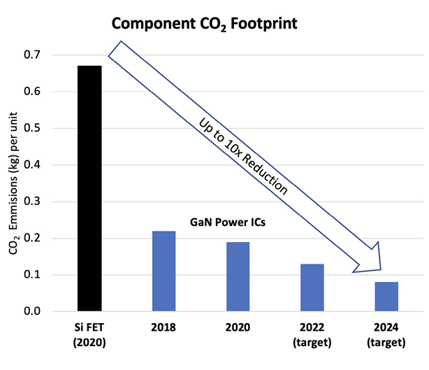
New GaN IC generation released every 12-15 months
Helping Customers Meet CO2 Goals – With GaN
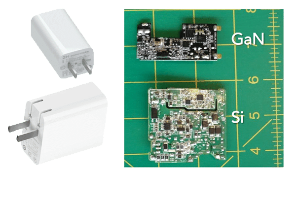
GaN power ICs enable power and charging systems to operate at up to 20x higher frequency than legacy silicon, which means up to 3x higher power, or 3x faster charging in half the size and weight, and with up to 40% energy savings ‘in use’. These application benefits bring commercial benefits to Navitas customers and end-users and deliver positive environmental benefits. Examples include:
a) High efficiency means lower temperature operation, minimizing or eliminating the need for heatsinks and larger cases.
b) Higher frequency GaN operation translates into fewer, smaller passive components (magnetics, filters, capacitors, etc.) and mechanical components (PCB, housing, heatsinks, etc.) reducing oil / refinement demand and lowering shipping costs and CO2 footprint.
c) Higher efficiency operation reduces in-use energy consumption.
Third-party total life-cycle analysis of 65 W charger upgrade from silicon to GaN power ICs.
![sibasev-gan-based-480x457[1]](https://navitassemi.com/wp-content/uploads/2023/11/sibasev-gan-based-480x4571-1.jpg)
Data Centers:
Save Over 10 million tons CO2 and $1.9 billion per year
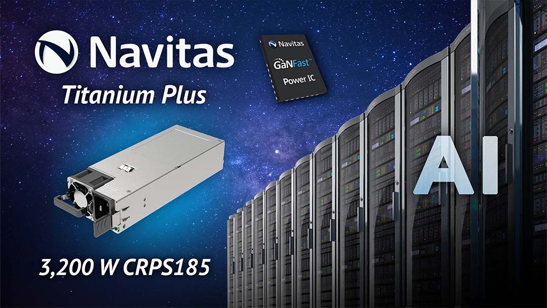
Upgrading from legacy silicon to high-efficiency GaN in the data center industry has the potential to reduce electricity use by up to 10% – an improvement that if applied across all data centers could reduce energy demand by over 15 TWh, save $1.9B in annual electricity costs and reduce CO2 by 10 Mtons – or the equivalent annual emissions of over 2 million gas-based passenger vehicles. 4 2


In support of climate action, the European Union has passed legislation (Directive 2009/125/EC, 2019 Annex) which states that new data center power supplies must meet the extreme 80 Plus ‘Titanium’ level of efficiency from January 1st, 2023. Compuware, the leader in high-efficiency server power has stated that “Navitas GaN is a breakthrough new technology that is enabling dramatic reductions in size, energy savings and power density.”5 Navitas’ new system platform design – CRPS185 3,200 W – exceeds the European requirement, with 40% higher power density than legacy silicon systems, and with a lower system price.6
Solar Adoption
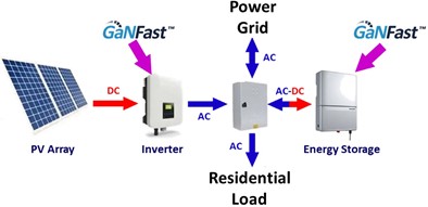
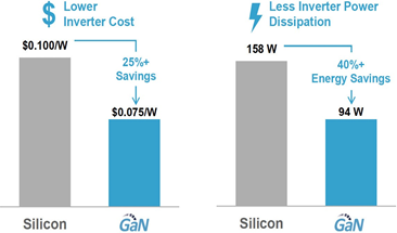
Every GaN IC Shipped Saves 4 kg CO2
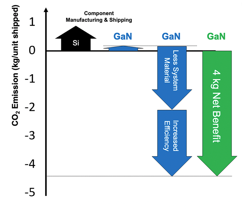
When we consider both the greatly-reduced manufacturing and transportation footprint, and the significant savings both to manufacture downstream products, and ‘in-use’ efficiency benefits, then we can present a per-unit net-benefit of upgrading from silicon to GaN power ICs.
Based on 2020 figures, every GaN power IC shipped reduces CO2 emissions by over 4 kg versus legacy silicon chips.8
Navitas is committed to corporate and industry-wide electrification innovations and reductions in CO2, as we strive to achieve the goals set out by the Paris Accord.
Navitas tracks GaN IC shipments and estimates hours of usage to calculate a running total of CO2 reductions.
Navitas’ expansion into the higher power markets of data center, solar and electric vehicles will accelerate these energy and CO2 savings.
Helping Customers Meet CO2 Goals – With SiC
SiC is the optimal material for high-power, high-voltage applications, such as solar inverters, motor drives and industrial applications. Here, the example is in the growing field of electric vehicles (EVs) and where SiC plays a very strong, enabling role in CO2 reduction. We begin with a simplified diagram showing the areas in an EV where SiC (and GaN) can play a role.
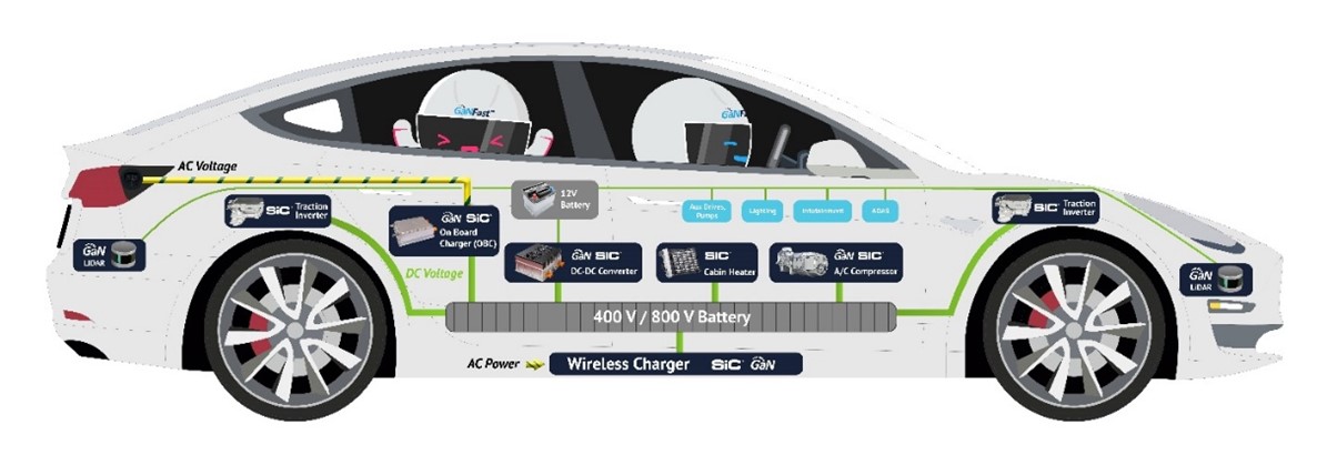
For a detailed analysis, we focus on an on-board charger (OBC) example, which converts power from 110/220 V AC mains to the high-voltage battery (800 V), can discharge (and invert) from the 800 V back to 110/220 V AC to power your home in case of a grid failure, and also provides a step-down DC-DC converter to power low-voltage (12 V) applications like navigation, seat motors, sensors, etc.
An 800 V system uses 1,200 V-rated devices, so Navitas’ G3R75MT12K SiC MOSFETs were the upgrade to Si IGBTs of the same voltage and similar RDS(ON) ratings. Overall, the SiC devices delivered 28% energy savings, with a CO2 footprint efficiency benefit of 34.5 kg saved, and dematerialization of 8 kg due to aluminum case / heatsink weight reduction.
Every SiC MOSFET Shipped Saves Over 25 kg CO2
As we upgrade from Si IGBTs to SiC FETs, the overall calculation method is the same but the result is very different. More electrical energy is required to grow a SiC boule than for Si, so on a per-unit basis, a SiC FET requires around 5x more energy, thus 5x more CO2. However, as SiC devices are used in high-power, long-lifetime applications, the cumulative benefits of CO2 savings due to system dematerialization (8.8 kg) and system efficiency increases (16.9 kg) dominate the result – with an overall 25.2 kg CO2 estimated benefit for SiC vs Si.9
Navitas tracks GaN and SiC shipments and estimates hours of usage to calculate a running total of CO2 reductions.
By the end of August 2023, over 100,000,000 GaN and 12,000,000 SiC power devices had been shipped, achieving a reduction of approximately 200,000 tons of CO2.
![average-miles[1]](https://navitassemi.com/wp-content/uploads/2023/11/average-miles1.jpg)

By 2050, GaN and SiC could save an estimated 6 Gtons/year CO2.

References and Citations
1 From Navitas information, DNV GL, EPA, IEA, International Renewable Energy Agency (IRENA). Derived from demand and energy efficiency CO2 reduction of 1.4 Gt; assumes a $0.12 / kWh cost of electricity and a carbon to energy ratio of 0.00071 tons / kWh, aligned with the EPA’s marginal emission rate.
2 Per EPA equivalencies calculator: https://www.epa.gov/energy/greenhouse-gas- equivalencies-calculator
3 The International Energy Agency’s (IEA’s) 2021 “World Energy Outlook” provides an indispensable guide to the opportunities, benefits and risks ahead at this vital moment for clean energy transitions. https://www.iea.org/reports/world-energy-outlook-2021 “Energy Efficiency 2021” is the IEA’s annual update on global developments in energy efficiency. The 2021 edition explores recent trends in energy efficiency markets at the economy-wide and sectoral levels, including developments in policy and investment. https://www.iea.org/reports/energy-efficiency-2021
4 Navitas estimate based on a) Navitas server/datacom forecast & AAAS data, b) $0.12/ kWhr, c) Si vs. GaN $/W and d) data centre loading profile.
5 Enphase Energy video testimonial at Navitas New York Investor Day, July 26th, 2021: https://navitassemi.com/enphase-customer-testimonial-navitas-semiconductor- investor-day-july-26th-2021-at-nasdaq-new-york/
6 Navitas CRPS185, 3,200 W AC-DC server power supply using GaNSafe power ICs, August 2023.
7 Navitas est. vs. Si-based 6.2kW residential inverters assuming GaN-based inverter enables 40% reduced power loss and 25% lower inverter costs
8 Up to 10x lower footprint: Navitas and Earth-Shift Global analysis. 4x lower for 2021, 10x lower by 2022 per life-cycle analysis. Up to 30% per Navitas and Earth-Shift Global estimated based on 65W charger per life-cycle analysis.
9 SiC device footprint per Navitas estimate from third-party Earth-Shift Global manufacturing and shipping estimate, plus Navitas analysis of 11 kW 3-in-1 on-board charger system platform design by Navitas EV Design Center. SiC G3R75MT12K vs Si IGBT 1,200V, 35 A. Use cases per US and EU models.
This sustainability report is part of Navitas’ overall Environmental, Social and Governance commitment. For more information, refer to ESG on the Navitas website.
This report uses the term ‘C02’ as an umbrella term for ‘CO2 equivalents’ (or CO2e) as defined by the EPA.
![energy-consumption-3[1]](https://navitassemi.com/wp-content/uploads/2022/08/energy-consumption-31.jpg)
![X-FAB_logo[1]](https://navitassemi.com/wp-content/uploads/2023/12/X-FAB_logo1.png)