GaN Power ICs
“GaNFast power ICs are the ultimate embodiment of next-generation power semiconductor technology in an easy-to-use, high-performance, extremely reliable format that is the dream of every power electronics designer.”
What is a GaN Power IC?
![GaNSense-evolution-3[1]](https://navitassemi.com/wp-content/uploads/2022/08/GaNSense-evolution-31.jpg)
A gallium nitride (GaN) power integrated circuit (IC) combines several power electronics functions onto a single GaN chip, to improve speed, efficiency, reliability and cost-effectiveness. In many cases, GaN power ICs are the enabling catalyst for advanced power-conversion topologies to transition from academic concepts to industry-proven mass production designs.
The key to improved performance is to create what approaches the ‘ideal switch’, i.e. a circuit building block that translates a minimum-energy digital signal into lossless power delivery.
Using lateral 650 V eMode GaN-on-Si technology, Navitas’ proprietary AllGaN™ process design kit (PDK) was created to enable the monolithic integration of GaN FET and GaN drive, plus logic and protection functions. The die can then be packaged into industry-standard, low-inductance, low-cost, 5×6 or 6×8 mm QFN packages for off-line AC or 400 V DC-input applications.
Both ‘single’ and ‘half-bridge’ GaN power ICs are available, with a broad range of power and functionality, and adaptable for a wide range of applications from tens of watts to kW in markets from mobile fast chargers, to data centers, consumer, renewables and EV / eMobility.
Half-bridge circuits are essential building blocks in the power electronics industry, used in everything from smartphone chargers to electric vehicles. High-frequency operation shrinks magnetics and other passive components to enable dramatic reductions in size, cost and weight while delivering faster charging. However, in half-bridge circuits, providing power and signal to a floating high-side switch at such frequencies have eluded the industry as silicon devices have been too slow and suffer from parasitic impedances between the driver and FET, high-capacitance silicon FETs and poorly performing level-shifter/isolators. GaN half-bridge power ICs including critical drive, logic, protection and power features eliminate the losses, costs and complexity associated with traditional half-bridge solutions.
The world’s first GaN power ICs deliver high frequency and high efficiency simultaneously, enabling a high-speed revolution in power electronics.
GaN power ICs enable up to 3x faster charging in half the size and weight of old, silicon-based power electronics, or 3x more power without a size or weight increase.
What is a GaNFast™ Power IC?
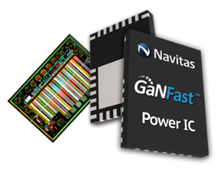
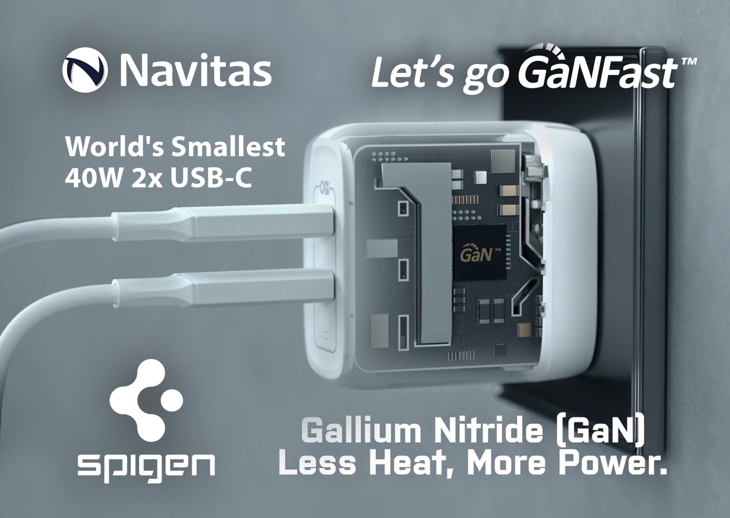
GaNFast is the trademark describing Navitas‘ proprietary GaN power ICs. GaNFast is also used in consumer-facing branding and co-operative marketing programs. Discover more about the 75+ GaN chargers in mass production at www.GaNFast.com . Sort by brand, power, weight and number and type of outputs to read reviews and buy your optimal GaN charger.
GaNFast power ICs are easy-to-use, high-speed, high-performance ‘digital-in, power-out’ building blocks. Integration enables virtually zero loss in turn-off because the gate drive loop has essentially zero impedance. In addition, turn-on performance can be controlled and customized for specific application requirements.
Who Invented the GaN Power IC?
While academic studies into low voltage GaN power ICs began around 2009 at HKUST, the industrialization of a robust, high-voltage GaN power IC platform was pioneered by Navitas, founded in 2014, with three of Navitas’ co-founders key players in the development of GaN power ICs.
The first high-voltage single and half-bridge GaN power ICs were demonstrated by Navitas at APEC 2015, with performance data up to 40 MHz. One year later, keynote speeches at APEC 2016 and PCIM 2016 cemented Navitas’ place as the home of GaN power ICs, with full qualification and release to mass production in 2018.
Are GaN Power ICs Patented?
Navitas has over 145 issued or pending patents, spanning a broad innovation range from semiconductor functional blocks (integrated gate drive, half-bridge, level-shifting, autonomous protection, etc.) and advanced low-inductance packaging, to high-frequency systems and application use cases.

How and Where Are GaN Power ICs Made?
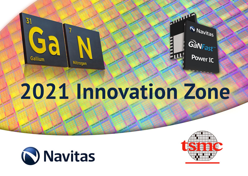
Navitas GaN power ICs are manufactured at TSMC’s wafer fab in Hsinchu, Taiwan. A standard silicon wafer is used as an inert mechanical baseplate and a very thin layer of GaN is epitaxially grown onto the top surface.
From there, standard CMOS processing techniques are followed including masking, etching, diffusion, sputtering, etc. to create a completed wafer containing thousands of GaN chips. While data-processing silicon chips require complex, sub-10 nm processing equipment, Navitas’ GaN-on-Si production uses cost-effective, and widely-available 250-350 nm equipment, making it very low capital expenditure (low ‘cap-ex’) manufacturing.
The wafers are then accurately sawn into individual dice (chips) and packaged into frequency-optimized QFN packages at Amkor and other partners.
What Are the Benefits of GaN Power ICs?
Faster: The integrated design of GaN power ICs makes them very easy to use. With simple ‘digital-in, power-out’ operation, layout and control is simple. Features such as dV/dt slew-rate control and under-voltage lockout ensure that GaN power ICs maximize the chance of first-time-right designs, which minimize time to market.
Greener: Due to small die-size, fewer manufacturing process steps and integrated functionality, GaN power ICs have a 10x lower CO2 footprint than silicon-based solutions. At a higher-level assembly, GaN-based chargers have half the manufacturing and shipping CO2-footprint of silicon designs.
How Do GaN Power ICs Enable Higher Efficiency at High Frequency?
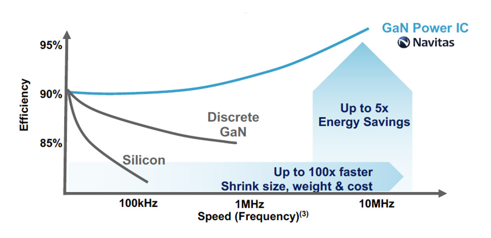
GaN brings low-charge (low-capacitance), low-loss benefits to single-switch circuits quasi-resonant flybacks, upgrading from a typical switching frequency of 50 kHz with old, slow silicon, to 200 kHz for discrete GaN.
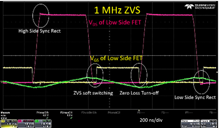
GaN power ICs amplify GaN’s frequency, density, and efficiency advantages in bridge topologies such as active-clamp flyback (ACF), CrCM totem-pole PFC and LLC. With a change from hard- to soft-switching topologies, the general loss equation for a primary FET can be minimized. The updated, simple equation results in improved efficiency at 10x higher frequencies.

How Fast is a GaN Power IC?
While silicon and discrete GaN designs struggle to achieve a few 100 kHz, all GaNFast power ICs are fully-rate at 2 MHz, with advanced work at Stanford University proving higher efficiency at 40 MHz than RF-rated silicon transistors.
Gallium Nitride (GaN) is a new ‘wide band gap’ semiconductor material with 100x faster switching and 20x improved performance over Silicon (Si).
Integration is key to minimize delays and eliminate parasitic inductances that have restricted the switching speed of Si and discrete GaN circuits. With propagation delays down to 5 ns, and robust dV/dt up to 200 V/ns, traditional 65-100 kHz converter designs can be accelerated to MHz and beyond [link to Bodo / Leonardo article]. Navitas’ GaNFast power ICs virtually eliminate all frequency-related losses making a 10-100x increase in switching frequencies a commercial reality.
For low-power chargers, new PWM control ICs have been introduced for high-frequency QR flyback up to 200 kHz from On Semiconductor (NCP1342) and up to 800 kHz for active-clamp flyback (ACF) from TI (UCC28782). For designs over 75 W, high-speed power factor correction (PFC) controllers include NCP1516 for CrCM boost up to 500 kHz, and NCP1680 for CrCM totem-pole up to 450 kHz.
For higher-power systems, where DoE Level IV / CoC Tier 2 standby specifications do not apply, then digital controllers like TI’s C2000 DSP enable systems such as 3,200 W AC-48V to run at 1 MHz.
How is a GaN Power IC Better Than a Discrete GaN Power FET?
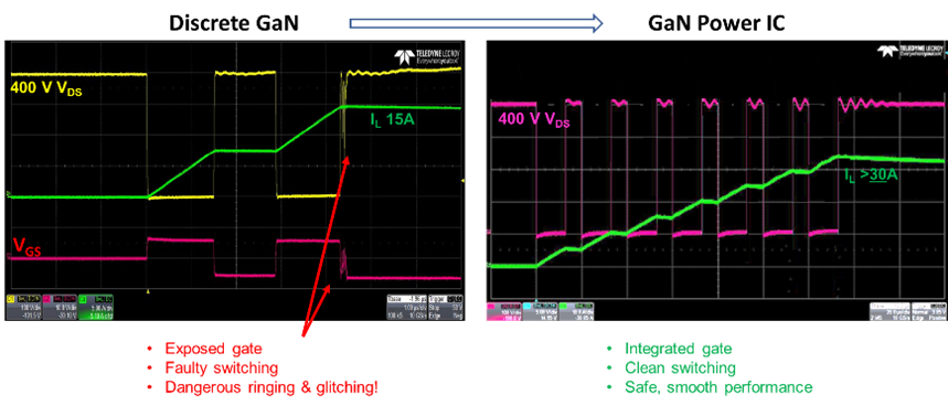
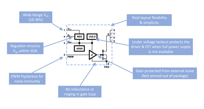
GaN power ICs are the ultimate in circuit design simplicity. Direct connection between the control IC’s digital PWM output and the GaNFast’s PWM input, with precise internal voltage regulation and no parasitic path to the GaN FET gate, ensures a simple, minimal component count, rugged solution.
Switching waveforms exhibit a true “textbook” feeling with very clean rising and falling edges and no ringing. Integration eliminates gate overshoot and undershoot, while zero inductance on-chip insures no turn-off loss. This lack of ringing or overshoot makes tight control of deadtime easy in half-bridge circuits.
Digital input means flexibility in design, with options for the GaN power ICs to be placed on the main board or daughtercard, close to or far from the control IC. Features like programmable dV/dt and UVLO ensure maximum flexibility, with confidence.
The erratic and lossy behavior of discrete GaN FETs is examined in more detail in a technical paper.
How Reliable are GaN Power ICs?
Navitas’ monolithically-integrated GaN power ICs entered the market in March 2018 with excellent device quality. As of May 3rd 2021, over 20,000,000 units had shipped, with 46,400,000,000 field device hours and zero (0) confirmed field failures.
Ongoing reliability monitoring (ORM) testing had reached 5,800,000,000 device hours at the same time, with a 0.16 FIT rate. For a real-time update on delivery and quality metrics, visit our Quality page.
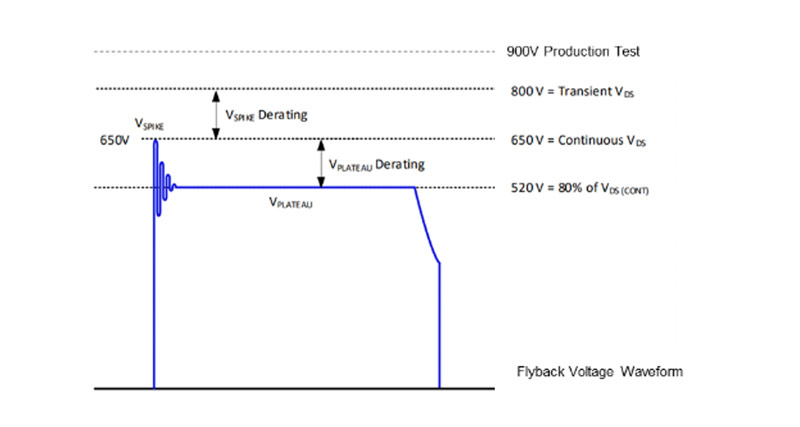
Navitas GaN power ICs also have a very high margin for voltage, with each part specified up to 800V and with a 900V production test on each device.
Where are GaN Power ICs Used?

GaN power ICs are used in power electronics, to convert from one voltage to another, e.g. from 110VAC from the AC wall outlet, to 20VDC to charge a laptop battery.
The applications and markets for GaN power ICs are extremely broad, from fast chargers for mobile smartphones (e.g. OPPO 50W PPS “Cookie” above) and laptops to data center power supplies, solar inverters, and EV / eMobility.
Customers include Dell, Lenovo, Xiaomi, Amazon and many more tier-1 companies.
Where Can I Buy GaN Power ICs?
GaN power ICs are immediately available from our specialized distribution partners worldwide, including DigiKey for 24/7 online information and ordering.
Where Can I Get Design and Application Support to Use GaN Power ICs?
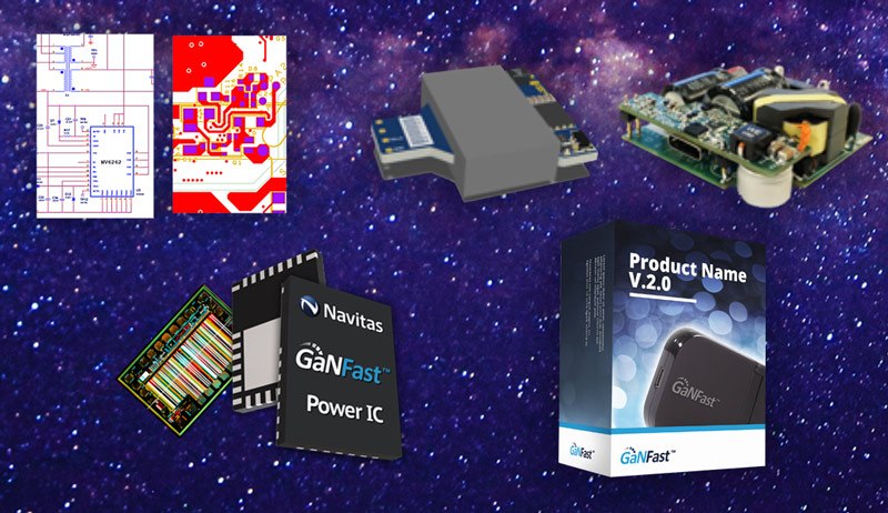
Join the GaN generation and partner with Navitas’ network of independent design houses to take your project from specification, through concept, prototype and on to mass production.


