Silicon Carbide:
The Facts

What is Silicon Carbide (SiC)?
Combining silicon (atomic number 14) and carbon (atomic number 6) with strong covalent bonds similar to those of diamond, silicon carbide (SiC) is a robust, hexagonal structure chemical compound offering wide band-gap semiconductor properties. Band-gap is the energy needed to free an electron from its orbit around the nucleus and, at 3.26 eV, the band-gap of silicon carbide is almost three times that of silicon, thus the designation ‘wide’ band-gap or WBG.
As band-gap determines the electric field that a material can withstand and the speed at which it can operate, the wider band-gap of silicon carbide enables the development of semiconductors that can operate at higher frequencies and higher voltages than conventional silicon. In addition, the chemical properties of silicon carbide give it a much better thermal conductivity and thermal stability than silicon, making it ideal for delivering consistent, reliable performance in high-voltage and high-temperature applications.

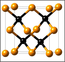
Silicon carbide crystalline structure (source: researchgate.net)
Why is Silicon Carbide (SiC) Important?
WBG semiconductors such as silicon carbide (SiC) are growing in importance because of their ability to offer significantly improved performance across a wide range of applications while reducing the energy and the physical space needed to deliver that performance when compared with conventional silicon technologies.
Why SiC Power Devices?
| Properties SiC vs Si | Performance of SiC Devices | Impact on Power Circuits |
|---|---|---|
| Breakdown Field (10x) | Lower On-state Voltage Drop (2-3X) | Higher Efficiency in Circuits |
| Thinner Epitaxial Layers (10-20x) | Faster Switching Speeds (100-1000X) | Compact Circuits |
| Higher Thermal Conductivity (3.3-4.5 W/cmK vs 1.5 W/cmK) | Higher Chip Temperatures (250-300°C instead of 125°C) | Higher Pulsed Power, Higher Continuous Current Densities |
| Band-gap (3X) (1016X Smaller n) | Lower leakage current, High Intrinsic Adiabatic Pulsed Current Level (3-10X) | High Temperature Operation, Higher Current Capability |
In some applications where silicon as a power conversion platform has hit its physical limits, SiC technologies are becoming essential, while in others the benefits of efficiency, switching speed, size, weight and cooler, high-temperature, high-voltage operation combine to make SiC increasingly attractive.
Silicon Carbide (SiC): History and Future
Silicon carbide does occur in nature as an extremely rare mineral known as moissanite, which was first found in 1893 in Arizona’s Canyon Diablo meteor crater. However, two years previous to this, American inventor Edward G. Acheson had accidentally discovered SiC, which he named carborundum, while looking for a way to produce artificial diamonds. In the following years Acheson patented his method for making silicon carbide powder and also developed the technology that is still used today to create SiC by reducing silica with carbon at high temperatures in an electric furnace.
Thanks to the hardness of the new compound – which, until the invention of boron carbide in 1929 was the hardest known synthetic material – the late nineteenth and early twentieth centuries saw SiC very quickly became popular on an industrial scale as a highly effective abrasive, an application for which it is still used today. In more recent years SiC has also been used as the basis for long-lasting ceramics used in automotive brakes and clutches.
The first decade of the twentieth century saw SiC used as detector diodes for early crystal radio sets, which in theory makes it the first commercially important semiconductor material. At this time it was also observed that the material would glow and change colour on application of an electric current, meaning it is also an early forerunner of the light emitting diode. Later that century the material’s electrical characteristics (a high resistance up to a certain threshold voltage dropping to a much lower resistance above that threshold) saw it deployed in lightning isolators for electric power distribution systems, in which columns of SiC pellets connected between high-voltage power lines and earth ensured lightning strikes passed to earth rather than along power lines.
However, it was the 1990s that saw significant R&D go into the creation of commercially viable SiC-based semiconductors. As a result of those efforts the first SiC Schottky diodes were launched in the early years of the 21st century and were followed by FETs for high-power switching. In 2008, the first commercial JFETs rated at 1200V were introduced to the market, followed in 2011 by the first MOSFETs rated at 1200V.
Since then, as the GeneSiC range of patent-protected silicon carbide devices illustrates, the range of SiC options available to system designers looking to reap the benefits of this WBG technology in their applications has grown significantly. The Navitas GeneSiC portfolio includes merged PiN Schottky (MPS) diodes with voltage ratings up to 1200 V, SiC junction transistors and MOSFETs capable of handling voltages up to 1,700 V and 6,500 V respectively, and PiN devices with ratings as high as 15,000 V.
Where are Silicon Carbide (SiC) Semiconductors Used?
SiC semiconductors are being deployed in a wide variety of use cases that demand robust high-voltage, high-performance operation from small form factor, high-power-density designs where stable and reliable operation is needed independent of temperature.
These include AC-DC rectifier and power factor correction (PFC) circuits, battery chargers, DC-DC converters, DC-AC inverters and frequency changers in applications ranging from electric vehicles (EVs) and traction control to data center architectures and solar inverters requiring 1000 – 1500 VDC operation.
The Navitas GeneSiC portfolio also supports 600-3300 V power transistors and rectifier products for demanding aerospace and oil drilling applications that require power-hungry control, communications, computing, propulsion and health monitoring systems.

The temperature robustness and radiation-hard properties of devices in the GeneSiC portfolio also allow these circuit elements to operate under extreme temperature and high radiation environments. The low on-state and switching losses of GeneSiC parts ensures much higher energy conversion efficiency, while offering a variety of features such as overload/short circuit protection, over-voltage protection, synchronization, over-temperature protection and the ability to run in parallel while providing low harmonic distortion, noise and EMI emissions.
How Does Silicon Carbide (SiC) Compare to Gallium Nitride (GaN)?
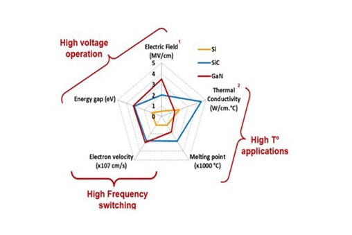
Compared to silicon that has a band-gap of 1.12 eV (electron-volts), GaN and SiC are compound semiconductors with band-gaps that are around three times higher at 3.39 eV and 3.26 eV respectively. This means that both can support higher voltages and higher frequencies, though there are a number of differences between the two technologies that impact how they work and where they are used.

Application design parameters for Si, GaN and SiC
One difference between GaN and SiC is speed in terms of electron mobility – how quickly electrons can move through the semiconductor material. At 2,000 cm²/Vs, GaN’s electron mobility is 30% faster than that of silicon, while SiC has an electron mobility of 650 cm²/Vs. These differences play a part in dictating the benefits that each technology offers a target application.
The higher electron mobility of GaN, for example, makes it much more suitable for high-performance, high-frequency applications, something that is further supported thanks to a very, very small percentage of the chip being actually consumed by the gate electrode. This ensures very low capacitance meaning it is easy to achieve higher frequencies (which is why GaN semiconductors are widely used in RF devices that switch in the gigahertz range).
SiC, on the other hand, with its higher thermal-conductivity and lower-frequency operation is more suited for higher-power applications including the higher-end voltages required in EVs and data centers, some solar-power designs, rail traction, wind turbines, grid distribution and industrial and medical imaging that do not always require high-frequency switching but do need higher-voltage operation and improved heat dissipation.
What is clear is that for power processing and fast charging, both GaN and SiC are superior materials to legacy silicon. 650V-rated GaN offers faster switching, integration, and lower costs, and is optimized for applications up to 20kW. The higher voltage and temperature properties of SiC make it optimal for devices over 1,000V and applications up to 20MW.