Introduction to
Wide Band-Gap
Semiconductors
What Defines a WBG Semiconductor?
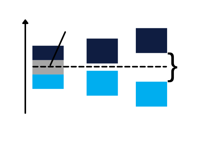
Physicists define the band-gap of a material as the difference in energy between the highest occupied state of the valence band (the band of electron orbits from which electrons jump when excited by the application of energy) and the lowest unoccupied state of the conduction band (the band to which those electrons can jump). The band-gap dictates the energy required for electrons to move from the valence band to the conduction band.

Legacy silicon, which has been the primary material for semiconductors since the 1950s, has a band-gap of 1.1 eV. The latest wide band-gap (WBG) semiconductors are those based on new and emerging materials that have band-gaps typically in the region of two to three times that of silicon.
What are the Benefits of WBG Semiconductors?
Silicon has been dominant for many years but is reaching its performance limits in a growing number of existing and emerging applications. Because WBG semiconductors can withstand higher electric fields they can sustain higher voltages. They can also operate at higher switching frequencies. The latter not only supports improved performance but also minimizes filtering requirements and allows the use of smaller external components (faster switching means energy is delivered in smaller packets and, therefore, less energy needs to be stored in the circuit’s passive and inductive devices).
When compared to legacy silicon these factors translate into a number of benefits including smaller, faster, more efficient and more reliable operation. Higher voltage capabilities open up opportunities in higher power designs while dramatically improved efficiencies enable the same performance in smaller form factors or allow improved performance in the same form factor. Efficiency also has an impact on weight and, ultimately, the carbon emissions associated with the operation of the target application.
Many devices based on WBG technologies also offer the benefit that they can operate at higher maximum temperatures than their legacy silicon counterparts.
What WBG Materials are Used for Semiconductors?
A number of materials including boron nitride, silicon dioxide and even diamond are all defined as WBG materials.

GaN and SiC are the two most prevalent WBG technologies in use today
However, the most prevalent WBG semiconductors today are those based on gallium nitride (GaN) and silicon carbide (SiC). The band-gaps of these materials are around three times greater than that of silicon, at 3.2 eV and 3.4 eV respectively.
What are the Differences Between GaN and SiC?
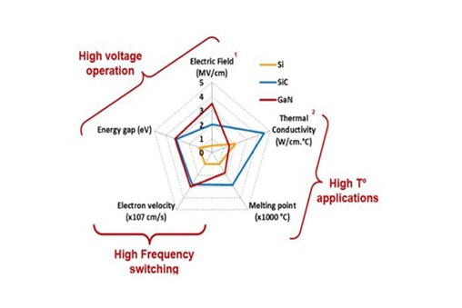
Compared to silicon that has a band-gap of 1.12 eV (electron-volts), GaN and SiC are compound semiconductors with band-gaps that are around three times higher at 3.39 eV and 3.26 eV respectively. This means that both can support higher voltages and higher frequencies, though there are a number of differences between the two technologies that impact how they work and where they are used.

Application design parameters for Si, GaN and SiC
One difference between GaN and SiC is speed in terms of electron mobility – how quickly electrons can move through the semiconductor material. At 2,000 cm2/Vs, GaN’s electron mobility is 30% faster than that of silicon, while SiC has an electron mobility of 650 cm2/Vs. These differences play a part in dictating the benefits that each technology offers a target application.
The higher electron mobility of GaN, for example, makes it much more suitable for high-performance, high-frequency applications, something that is further supported thanks to a very, very small percentage of the chip being actually consumed by the gate electrode. This ensures very low capacitance meaning it is easy to achieve higher frequencies (which is why GaN semiconductors are widely used in RF devices that switch in the gigahertz range).
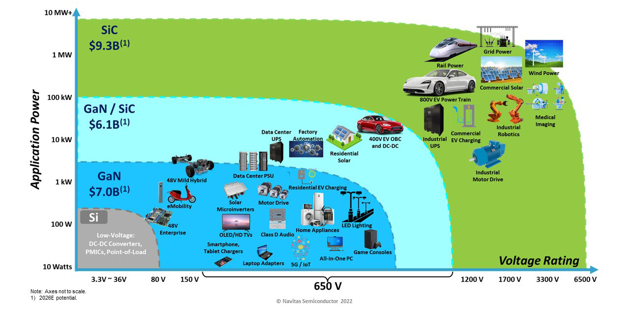
SiC, on the other hand, with its higher thermal-conductivity and lower-frequency operation is more suited for higher-power applications including the higher-end voltages required in EVs and data centers, some solar-power designs, rail traction, wind turbines, grid distribution and industrial and medical imaging that do not always require high-frequency switching but do need higher-voltage operation and improved heat dissipation.
What is clear is that for power processing and fast charging, both GaN and SiC are superior materials to legacy silicon. 650V-rated GaN offers faster switching, integration, and lower costs, and is optimized for applications up to 20kW. The higher voltage and temperature properties of SiC make it optimal for devices over 1,000V and applications up to 20MW.
WBG Semiconductor Applications
GaN + SiC: The Future of Power Semis

What is the Potential for WBG Semiconductors?
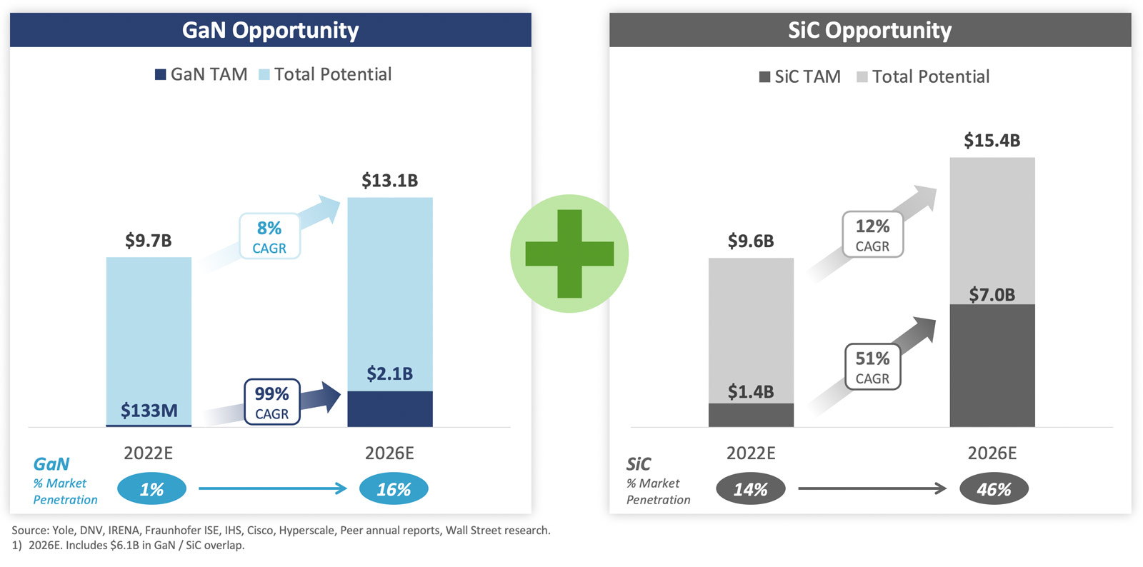
The potential market for WBG semiconductors is already significant and growing rapidly as companies look to replace legacy silicon in existing applications and to harness the power of GaN and SiC in new and emerging designs where silicon cannot compete. At Navitas we estimate the combined market opportunity for GaN and SiC power technologies to be over $20B a year by 2026.
