Gallium Nitride:
The Facts

What is Gallium Nitride (GaN)?
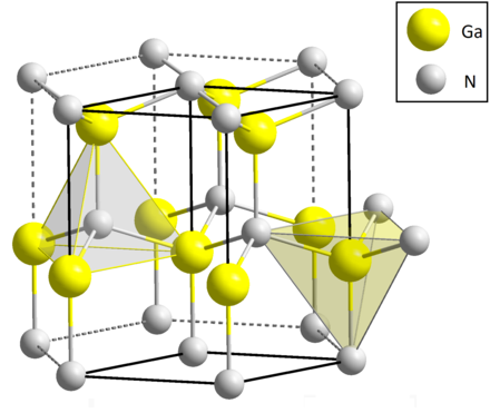
Combining gallium (atomic number 31) and nitrogen (atomic number 7), gallium nitride (GaN) is a wide bandgap semiconductor material with a hard, hexagonal crystal structure. Bandgap is the energy needed to free an electron from its orbit around the nucleus and, at 3.4 eV, the bandgap of gallium nitride is over three times that of silicon, thus the designation ‘wide’ bandgap or WBG.
As bandgap determines the electric field that a material can withstand, the wider bandgap of gallium nitride enables the development of semiconductors with very short or narrow depletion regions, leading to device structures with very high carrier density. With much smaller transistors and shorter current paths, ultra-low resistance and capacitance is achieved, enabling speeds that are up to 100x faster.
The bottom line is that GaN technology can handle larger electric fields in a much smaller form factor than conventional silicon while delivering significantly faster switching. In addition, GaN technologies can operate at higher maximum temperatures than their silicon-based counterparts.
Why is Gallium Nitride (GaN) Important?
Gallium nitride (GaN) is growing in importance because of its ability to offer significantly improved performance across a wide range of applications while reducing the energy and the physical space needed to deliver that performance when compared with conventional silicon technologies. In some applications where silicon as a power conversion platform has hit its physical limits, gallium nitride technologies are becoming essential, while in others the benefits of efficiency, switching speed, size and high-temperature operation combine to make GaN increasingly attractive.
As global need for energy increases, a move to GaN technology will help to meet demand while keeping carbon emissions to a minimum. Indeed, GaN design and integration has been shown to deliver next-generation power semiconductors with a carbon footprint ten times lower than older, slower silicon chips. To further support the case for GaN, it is estimated that a worldwide Si-to-GaN data center upgrade would reduce energy loss by 30-40%, which would translate as saving over 100 TWhr and 125 Mtons of CO2 emissions by 2030.
![energy-consumption-3[1] Sustainability](https://navitassemi.com/wp-content/uploads/2022/08/energy-consumption-31.jpg)
![energy-consumption-3[1]](https://navitassemi.com/wp-content/uploads/2022/08/energy-consumption-31.jpg)
Gallium Nitride (GaN): History and Future
Gallium does not exist in elemental form in nature. It is typically derived as a by-product from the smelting of bauxite ore into aluminum and from the processing of sphalerite ore for zinc, so has a very low extraction and refinement carbon footprint.
Over 300 tons of gallium are produced every year, with over a million tons estimated in reserves around the world. As it is a processing by-product, it is relatively low cost, at around $300/kg which is 200x lower than gold, at around $60,000/kg.
Gallium’s existence was predicted in 1871 by Dmitri Mendeleev and discovered only a few years later in Paris in 1875 by Paul-Émile Lecoq de Boisbaudran, who named it after the Latin Gallia (Gaul) for his home country of France. In its pure form, gallium nitride has a melting point of only 30 °C (86 °F) so will melt in a person’s hand at normal human body temperature.


It was to be a further 65 years before gallium nitride was first synthesized and not until the 1960s that single crystal films of gallium nitride were grown. Now, as a compound, GaN has a melting point of over 1,600 °C, that’s 200 °C higher than silicon.
In 1972 GaN-based LEDs were created (using gallium nitride doped with magnesium). This was a significant milestone because, while initially not bright enough for commercial use, these were the first LEDs capable of emitting a blue-violet color. A method for producing higher brightness blue LEDs was patented in 1991 and two years later high-brightness blue LEDs were demonstrated.
The commercial availability of high-brightness blue LEDs was an inflexion point for the electronics industry. By adding a phosphor coating it was possible to create white LEDs capable of replacing inefficient incandescent lighting. Adding red and green LEDs gave the primary colors needed to create a working, LED-based display. From the first LED-backlit LCD TVs to the latest OLED screens, this ensured the complete destruction of the cathode ray tube (CRT) television and monitor market as well as the demise of the related Si ‘deflection transistor’.
Gallium nitride, therefore, is the enabling technology behind the high-resolution color screens we have in our TVs, phones, tablets, laptops and monitors. And adding to the photonics story, GaN is also deployed in blue lasers (most notably those used to read discs in Blu Ray players).
Outside of photonics, while GaN transistors were demonstrated in 1993 it was around 2004 that that the first GaN HEMT (high electron mobility transistor) transistors became commercially available. These were typically used in RF infrastructure applications that needed their high efficiency, high-voltage capabilities. A few years later, in 2008, saw the promotion of GaN MOSFETs (formed on a silicon substrate) – though adoption was minimal due to circuit complexity and lack of high-frequency eco-system components.
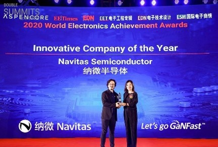
Navitas Semiconductor was formed in 2014 with a mission to enable a high-speed revolution in power electronics by providing GaN power ICs that can deliver the benefits of this wide bandgap (WBG) technology to the widest possible range of applications. In 2018 EETimes selected the company in its prestigious ‘Silicon 60’ startup ranking and in 2019 Frost and Sullivan recognized the company for its unique vision and system-level approach to enabling next-generation GaN-based power systems. Also in 2019, Navitas was awarded the Shanghai Zhangjiang 895 and Zhangjiang Science City ICV Pioneer Alliance ‘Innovation Star’, followed in 2020 by both the ‘Semiconductor Design Innovation Excellence Award’ from the China Communication Industry Association (CCIA) and the Aspencore ‘Outstanding Innovative Company of the Year’ award.
In the same year the company announced that it had been issued with over 100 patents in gallium nitride devices and applications.
Navitas has continued to develop its family of GaNFast power ICs, which, unlike most Si and earlier discrete GaN devices, are provided in very small, low-profile, surface-mount QFN packages eliminating speed-limiting, lossy discrete drive and protection circuits, and shrinking printed circuit (PCB) area.
By 1st April, 2021, Navitas has shipped 18,200,000 gallium nitride power ICs with zero failures.
To see the latest GaN power IC shipment and quality information, visit our Quality page.
Where are Gallium Nitride (GaN) Semiconductors Used?
Gallium nitride has long been used in the production of LEDs and RF components but is now moving to mainstream acceptance in a growing number of power switching and conversion applications. Here GaN-based ICs can address demands to improve system performance and efficiency, save space and deliver reliable operation at higher temperatures.
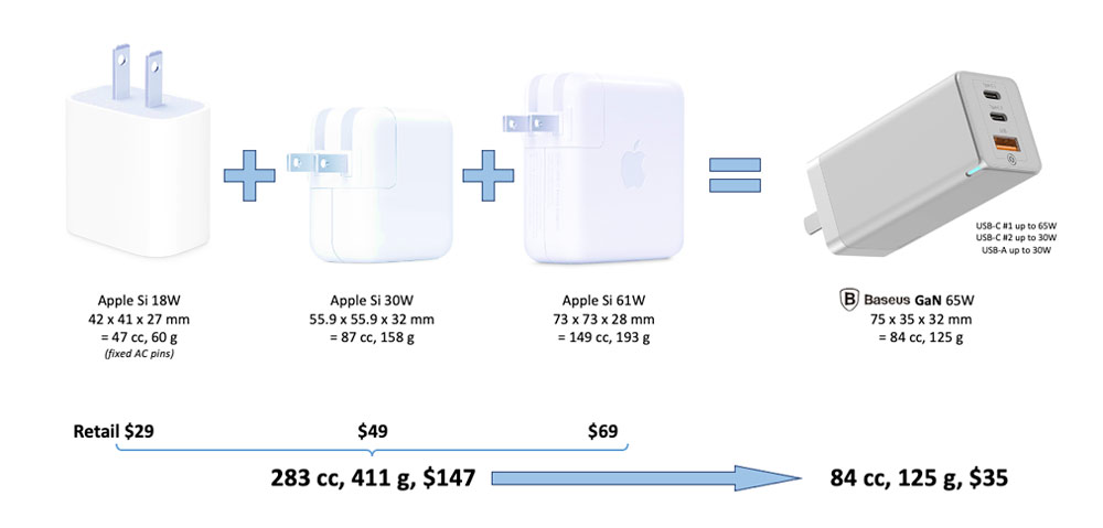
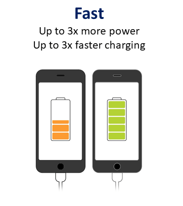
Within phones and laptops GSM and WiFi signals are transmitted and received using GaN RF devices, while the chargers and adaptors that power these devices increasingly incorporate GaN. Indeed, the largest market for power GaN is currently in mobile fast charging where GaN power ICs can enable three times faster charging in adaptors that are half the size and weight of slow, silicon-based designs. What’s more, for single-output chargers, GaN retail launch pricing is around half that of previous best-in-class silicon chargers and as much as three times lower in the case of multi-output chargers.

Gallium nitride power semiconductors are also being deployed in data center servers. As data center traffic accelerates, silicon’s ability to process power effectively and efficiently hits ‘physical material’ roadblocks. As a result, the old, slow, silicon chip is overtaken by high-speed gallium nitride ICs.
The consolidation of data center hardware, a new HVDC architecture approach and the proven reliability of mass-production, highly-integrated GaN power ICs enable major improvements in efficiency. It is estimated that a worldwide Si-to-GaN data center upgrade would reduce energy loss by 30-40%, which would translate as saving over 100 TWhr and 125 Mtons of CO2 emissions by 2030. Deploying GaN, therefore, represents another step towards carbon ‘Net-Zero’ goals for the data center industry.
Why is Gallium Nitride (GaN) Superior to Silicon?
Gallium Nitride (GaN) is a ‘wide bandgap’ (WBG) material, the bandgap being the energy required to free an electron from its orbit around the nucleus and allow it to move freely through the solid. This, in turn, determines the electric field that the solid is able to withstand.
Silicon (Si) has a bandgap of 1.1 eV, while GaN has a bandgap of 3.4 eV. As the WBG material allows high electric fields, depletion regions can be very short or narrow, so device structures can have higher carrier density and be packed very densely. For example, a typical 650 V lateral GaN transistor can support over 800 V and has a drain drift region of 10-20 µm, or about 40-80 V/µm. This is substantially above the theoretical limit of silicon, which is around 20 V/µm. However, it is still well short of the bandgap limit of about 300 V/µm, leaving substantial room for generational improvements in lateral GaN devices in the future.
In device-level terms, the figure of merit derived from the product of normalized on resistance (RDS(ON)) and gate charge (QG) can be from five times to twenty times better than silicon, depending on implementation. By facilitating much smaller transistors and shorter current paths, ultra-low resistance and capacitance is achieved and switching speeds are up to one hundred times faster.
In order to fully exploit GaN power IC capability, the rest of the circuit must also be able to run effectively at higher frequencies. In recent years, control ICs have been introduced to take switching frequencies from 65-100 kHz up to 1 MHz+, with new controllers in development. Microcontrollers and digital signal processors (DSPs) can also be used to implement today’s soft switching circuit topologies, while a broad range of magnetic materials that are optimized for the 1-2 MHz range are now available.
GaN power ICs combine frequency, density, and efficiency advantages in half-bridge topologies such as active clamp flyback, totem-pole PFC and LLC. With a change from hard- to soft-switching topologies, the general loss equation for a primary FET can be minimized, leading to improved efficiency at 10x higher frequencies.
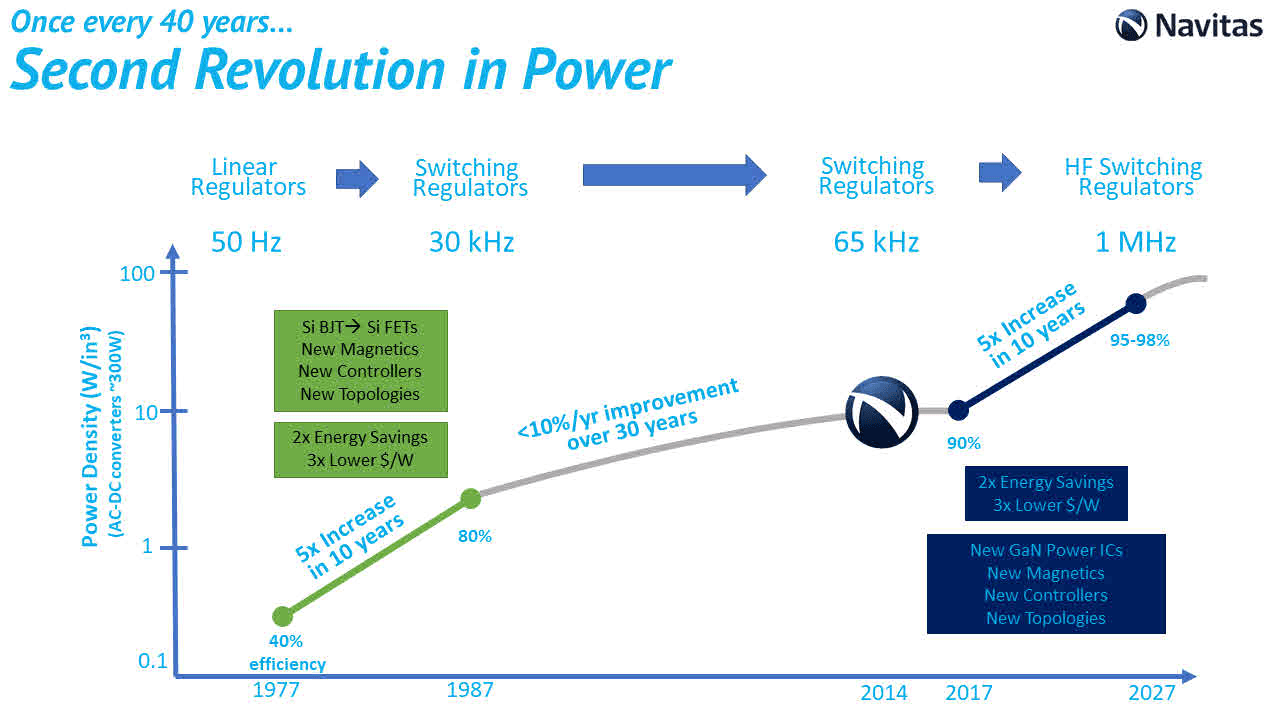
With record-breaking performance, gallium nitride power ICs are the catalyst for a second revolution in power electronics.
How Does Gallium Nitride (GaN) Compare to Silicon Carbide (SiC)?
Compared to silicon that has a band-gap of 1.12 eV (electron-volts), GaN and SiC are compound semiconductors with band-gaps that are around three times higher at 3.39 eV and 3.26 eV respectively. This means that both can support higher voltages and higher frequencies, though there are a number of differences between the two technologies that impact how they work and where they are used.
Application design parameters for Si, GaN and SiC
One difference between GaN and SiC is speed in terms of electron mobility – how quickly electrons can move through the semiconductor material. At 2,000 cm²/Vs, GaN’s electron mobility is 30% faster than that of silicon, while SiC has an electron mobility of 650 cm²/Vs. These differences play a part in dictating the benefits that each technology offers a target application.
The higher electron mobility of GaN, for example, makes it much more suitable for high-performance, high-frequency applications, something that is further supported thanks to a very, very small percentage of the chip being actually consumed by the gate electrode. This ensures very low capacitance meaning it is easy to achieve higher frequencies (which is why GaN semiconductors are widely used in RF devices that switch in the gigahertz range).
SiC, on the other hand, with its higher thermal-conductivity and lower-frequency operation is more suited for higher-power applications including the higher-end voltages required in EVs and data centers, some solar-power designs, rail traction, wind turbines, grid distribution and industrial and medical imaging that do not always require high-frequency switching but do need higher-voltage operation and improved heat dissipation.
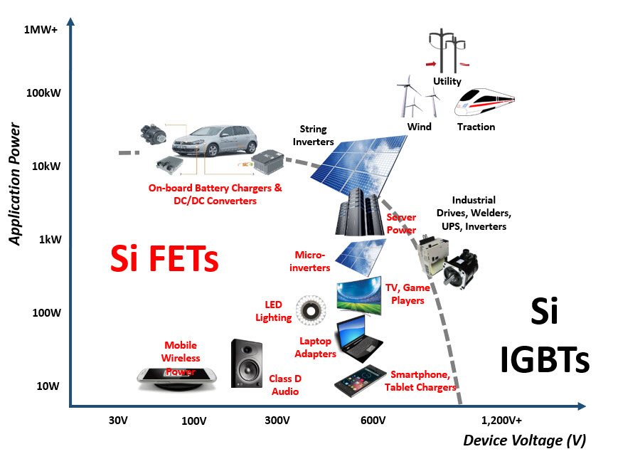
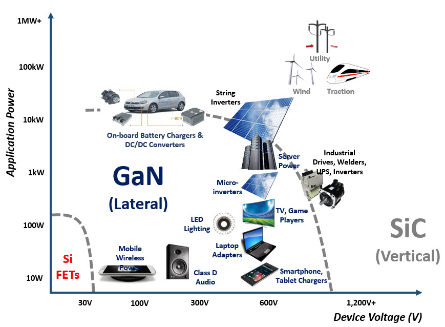
What is clear is that for power processing and fast charging, both GaN and SiC are superior materials to legacy silicon. 650V-rated GaN offers faster switching, integration, and lower costs, and is optimized for applications up to 20kW. The higher voltage and temperature properties of SiC make it optimal for devices over 1,000V and applications up to 20MW.
The Wide Band-Gap Landscape
GaN’s wide band-gap allows power applications with voltages between 100 V and 600 V to use smaller, more efficient chips, reducing costs and carbon emissions. SiC, with higher thermal conductivity, is only suited for the highest power applications that require large heat dissipation. Current flow is another critical difference; SiC is a ‘vertical’ device which is optimized for high power only, while Navitas’ GaN, for example, has a ‘lateral’ structure that makes monolithic (‘same chip’) integration possible. The lateral structure enables GaN power ICs to integrate power FETs with drive, logic, protection, sensing and control.
How do Gallium Nitride (GaN) Power ICs Improve Fast Charger Design?
If we take the common application example of a phone or laptop charger, low resistance and low capacitance enabled by GaN technology translates to higher charging efficiencies, so more of the power is delivered to the battery, charging it faster (instead of burning up that energy as heat which warms the charger). Moreover, faster switching means that the charger can deliver more power to the battery with a dramatically smaller size and weight as the energy-storing passive components can be shrunk dramatically (as they store much less energy in each switching cycle).
By supporting higher power densities and switching frequencies, gallium nitride (GaN) ICs not only minimize the size of the power semiconductor itself but also provide designers with a route (depending on the power supply topology) to reducing the size of the main transformer, EMI filter components, output capacitors and bulk capacitors.
As different components shrink, we have a ‘Manhattan skyline’ of tall and short components, soldered to a main printed-circuit board (PCB). This leaves large airgaps above and around the smaller components – space which can be used for new thinking and 3D mechanical designs that optimize power density.
A gallium nitride power IC monolithically-integrates GaN power (FET) and GaN drive plus control and protection in a single SMT package. These GaNFast™ power ICs become easy-to-use, high-speed, high-performance ‘digital-in, power-out’ building blocks. Integration enables virtually zero loss in turn-off because the gate drive loop has essentially zero impedance. In addition, turn-on performance can be controlled and customized for specific application requirements.
For the designer, ‘ease-of-use’ translates very quickly into faster prototyping and maximizing ‘first-time-right’ designs, and robust, high-quality performance means short qualification time. These factors accelerate time-to-market and time-to-revenue metrics.
GaN fast chargers have been released by tier-1 OEMs such as Dell, Lenovo, Samsung, Xiaomi, LG and OPPO plus a broad range of aftermarket companies including Belkin, Anker, AUKEY, Hyper and Baseus.



What is a GaN Power IC?
![GaNSense-evolution-3[1] GaN Power IC](https://navitassemi.com/wp-content/uploads/2022/08/GaNSense-evolution-31.jpg)
GaN or NGa? Gallium Nitride in English and Chinese
Whether you are in Boston or Beijing, San Jose or Shanghai, you’ll hear the pronunciation GaN time and time again in conversations about everything from fast charging of laptops to the latest renewable energy designs.
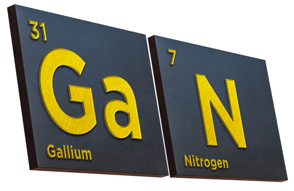
It’s interesting to note, that while the US and UK talk of gallium nitride, in China the correct way to refer to this revolutionary material is actually as a nitride of gallium. So, while Chinese engineers may still talk of GaN, when they write down the formula it is with the nitrogen symbol preceding the gallium atom, or NGa. In addition, the Chinese version of the formula contains three symbols – one each for gallium (镓) and nitrogen (氮) and a 化 to connect them.
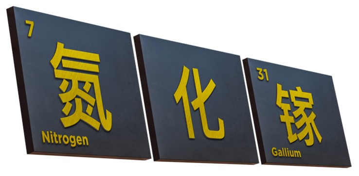
As a leader in gallium nitride technology, Navitas has already shipped millions of GaN devices, many of them to OEMs in China. In support of its growing presence in the region, the company also recently created “Little GaN Stars”, twins XiaoDan (Little Nitrogen) and XiaoJia (Little Gallium) to represent, respectively, the two elements of this high-efficiency material.

Now a regular feature on Navitas booths at trade shows and events throughout Asia, these characters stand next to each other with XiaoJia to the left of XiaoDan, reflecting the correct Chinese notation for gallium nitride.
