Markets and Technology
In applications from 20 W to 20 MW, and with device voltages from 650 V to 6.5 kV, GeneSiC silicon carbide (SiC) MOSFETs and Schottky MPS™ diodes drive high-speed, high-efficiency power conversion across diverse markets including EV, industrial automation, solar, wind, grid, motor drives and defense. High-volume, high-quality shipments ensure application performance, reliability and uptime availability.

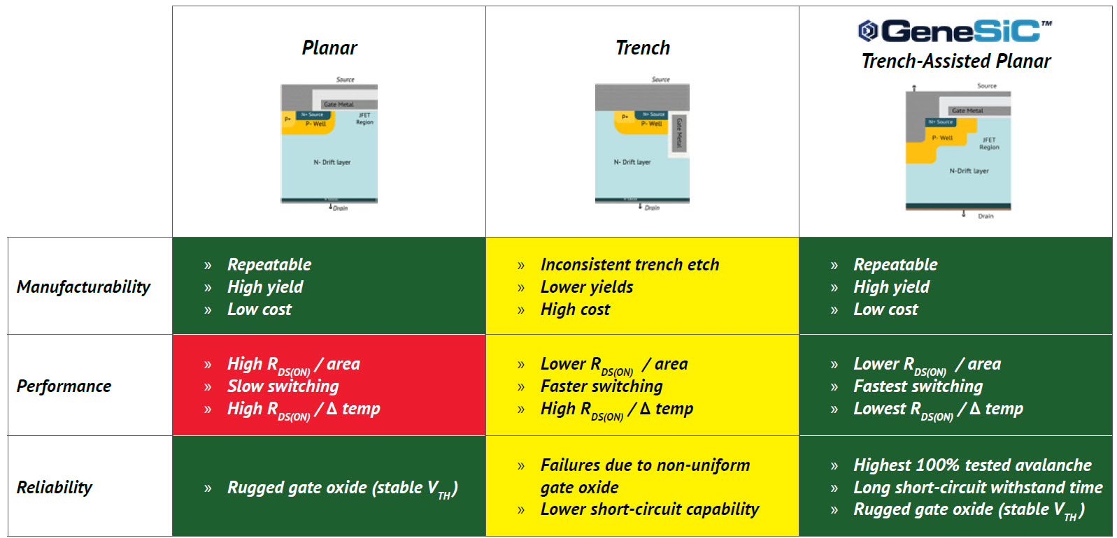
Trench-Assisted Planar Gate: No-Compromise Technology
SiC MOSFETs offer superior conductivity and switching performance compared to silicon (Si) due to their ‘wide bandgap’ characteristics and high electric-field strength. However, traditional designs using legacy planar or trench techniques must compromise between manufacturability, performance, and/or reliability.
GeneSiC’s patented trench-assisted planar gate design is a no-compromise, next-generation solution; high-yield manufacturing, fast and cool operation, and extended, long-life reliability.
Cool. Fast.
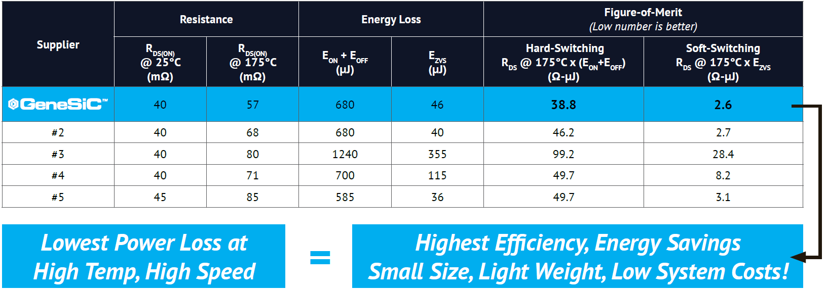
Efficient, cost-effective power conversion relies on a comprehensive understanding of modern circuit topologies and high-speed (frequency) switching techniques. There are two main device factors;
• How well does the MOSFET conduct current (measured in RDS(ON) )?
• How efficiently does the device ‘switch’ (measured by energy loss, or EXX )?
For each question, we must understand the answer in both ‘hard-switch’ and ‘soft-switch’ topologies, and under tough hightemperature and high-speed conditions. Combined, a high-temperature, high-speed (frequency) figure-of-merit (FoM) is critical for system performance and reliability.
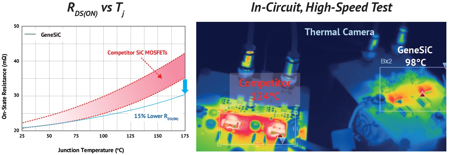
GeneSiC vs. competitor SiC FET
» 1200 V, 20 mΩ, TO-247-4L
» Higher drain current
» Lower conduction losses
» Cooler operation
GeneSiC vs. competitor SiC FET
» 1200 V, 40 mΩ, D2pak in half-bridge
» 150 kHz switching = ~10x faster than Si IGBT
» 30% lower FET loss vs. other SiC
» 25°C cooler operation = 3x longer lifetime
Rugged.
Gen 3 ‘Fast’ SiC MOSFETs
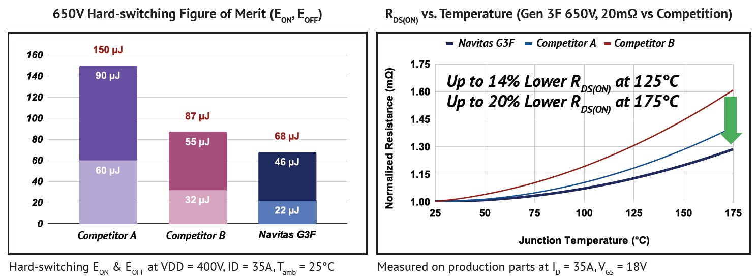
GeneSiC’s 3rd generation of fast SiC MOSFETs improves switching performance and system efficiency:
- Optimized EMI
- Low VF and QRR
- Robust body diode
- Cooler operation
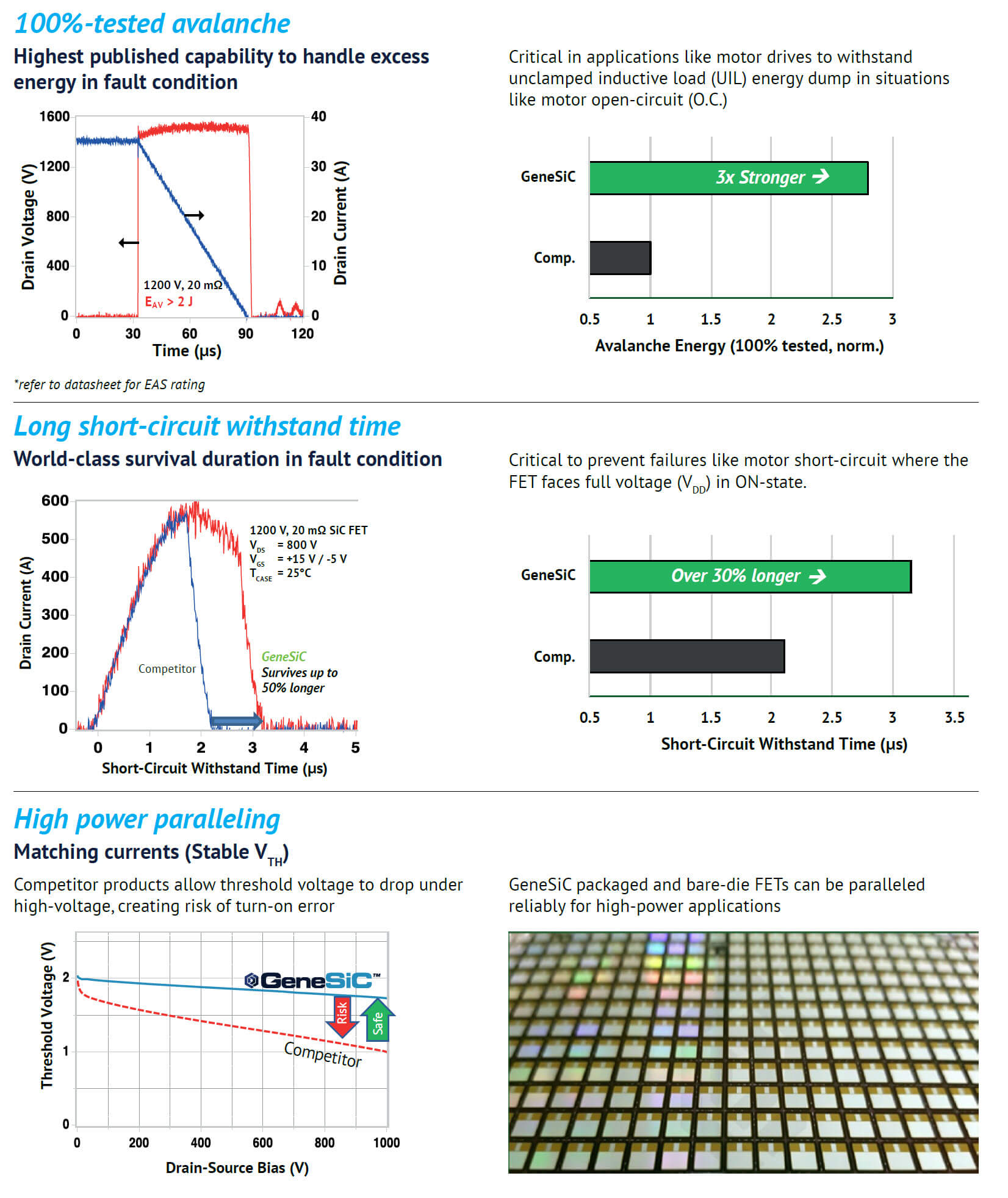
- 100% avalanche (UIL) tested
- Ultra-low RDS(ON) vs. temperature dependency
Target applications include EV charging, solar inverters, data center and telecom power supplies, and energy storage systems (ESS).
4.5kW, 137W/in3, 97% efficiency AI data center PSU

Gen 3 Fast SiC MOSFET: G3F45MT06L (650V, 40mΩ TOLL)

Interleaved CCM TP PFC with G3F SiC MOSFETs & GaNSafe Power ICs
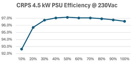
• Exceeds Titanium efficiency (>97%)
• Hold up time: 10ms @4200W
• EMI: Class A with >6dB
TOLL Package for high speed, high efficiency, and high-power density systems
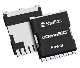
- Extremely low package inductance of 2nH
- Small footprint with 30% savings in PCB area compared to D2PAK
- Lower height profile, with 60% lower volume than D2PAK
- Excellent thermal properties, with 9% lower RTHJC compared to D2PAK
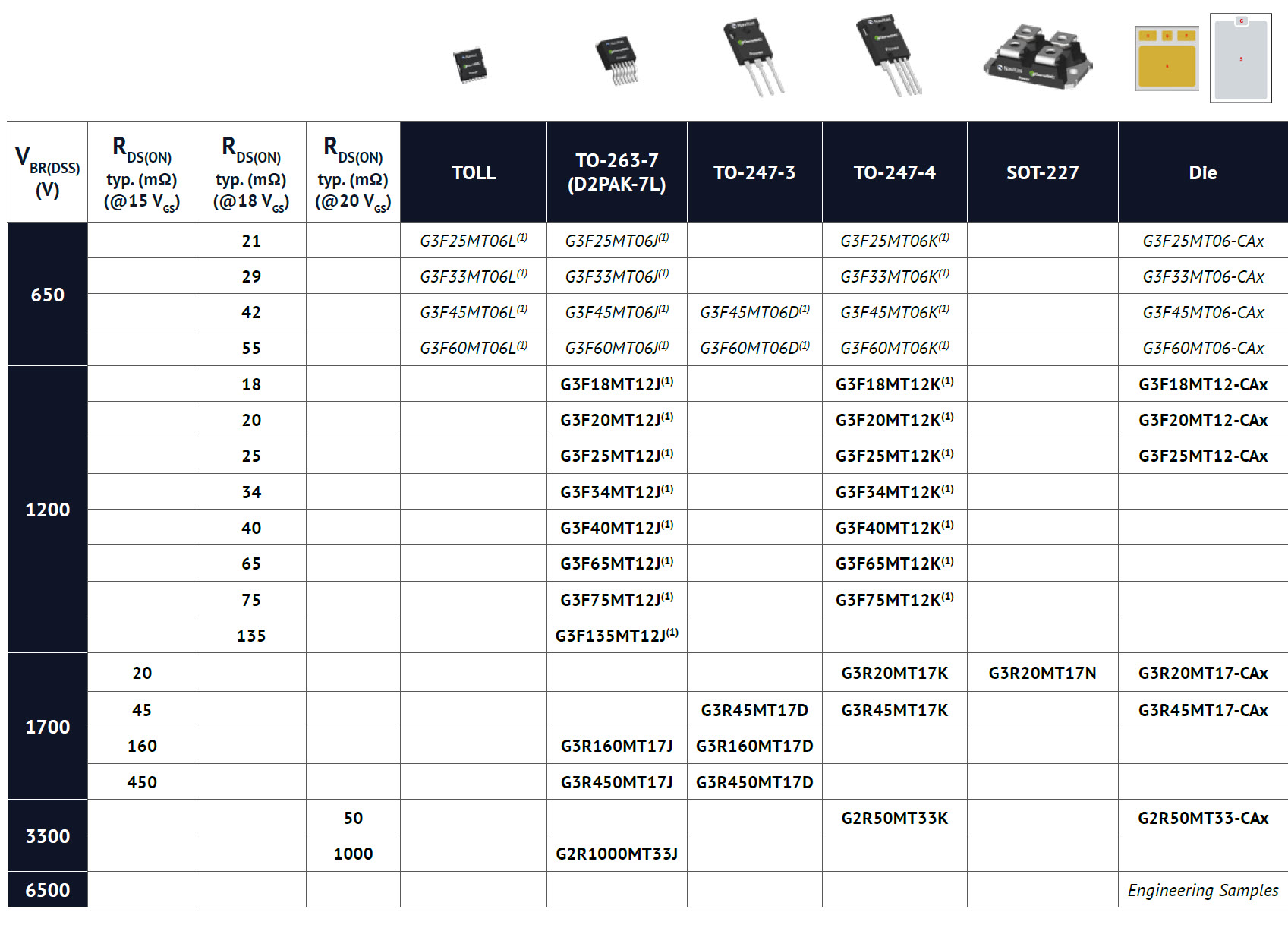
Widest Range of SiC MOSFETs 650 V – 6.5 kV
To access product datasheets, models, and to order parts, please click here.
(1) Automotive qualified
Bare Die Metallization – CAx (-CAL Aluminum, -CAU Gold)
Typical Circuits


Built to the Highest Level of Reliability
High-voltage pioneers
Robust, high-voltage, high-efficiency SiC MOSFETs, critical for reliable, harsh-environment, high-power applications.
Unique, advanced, integrated 6.5 kV technology
» Double-implanted metal oxide semiconductor (DMOSFET)
» Monolithically-integrated Junction barrier Schottky (JBS) rectifier
» Superior high-power performance
» Temperature independent switching
» Fast (low switching loss) and cool (low conduction losses)
» Longer-term reliability
» Easy-to-parallel for high power (VTH stability)


High power modules & die sales
GeneSiC SiCPAK™ modules and bare-die enable expanded applications ranging from 10s kW to MW in rail, EV,
fast charging, industry, solar, wind and energy storage.

robustness, while meeting industry-standard footprint with pin-to-pin combability.
- Epoxy-Resin Potting Technology for High Reliability
- Improved Temperature Cycling
- Improved Power Cycling
- ‘Gen3 Fast’ SiC MOSFETs with Industry-Leading Current Density (A/mm2)
- Optimized Low-Inductance Design with Industry-Standard Press-Fit Connections
with built-in NTC and Pin-to-Pin Compatibility


650 V MPS™ Diodes
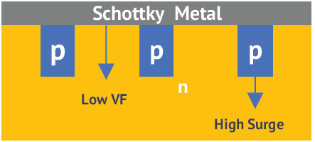
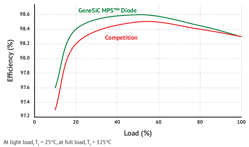
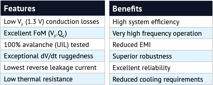
GeneSiC’s new 5th-generation 650 V Merged-PiN Schottky (MPS™) diodes integrate a unique PiN Schottky structure, delivering ‘low-built-in Voltage-Biasing’ (“low knee”) for highest efficiency across all load conditions with superior robustness. Applications include PFC in server/telecom power supplies, industrial motor drives, solar inverters, LCD/LED TVs, and lighting.
Merged-PiN Schottky (MPS™) with Low-Built-In Voltage-Biasing Technology

Superior Figure-of-Merit (FoM) Drives High Efficiency
3 kW Interleaved Boost PFC
Typical Application Circuits

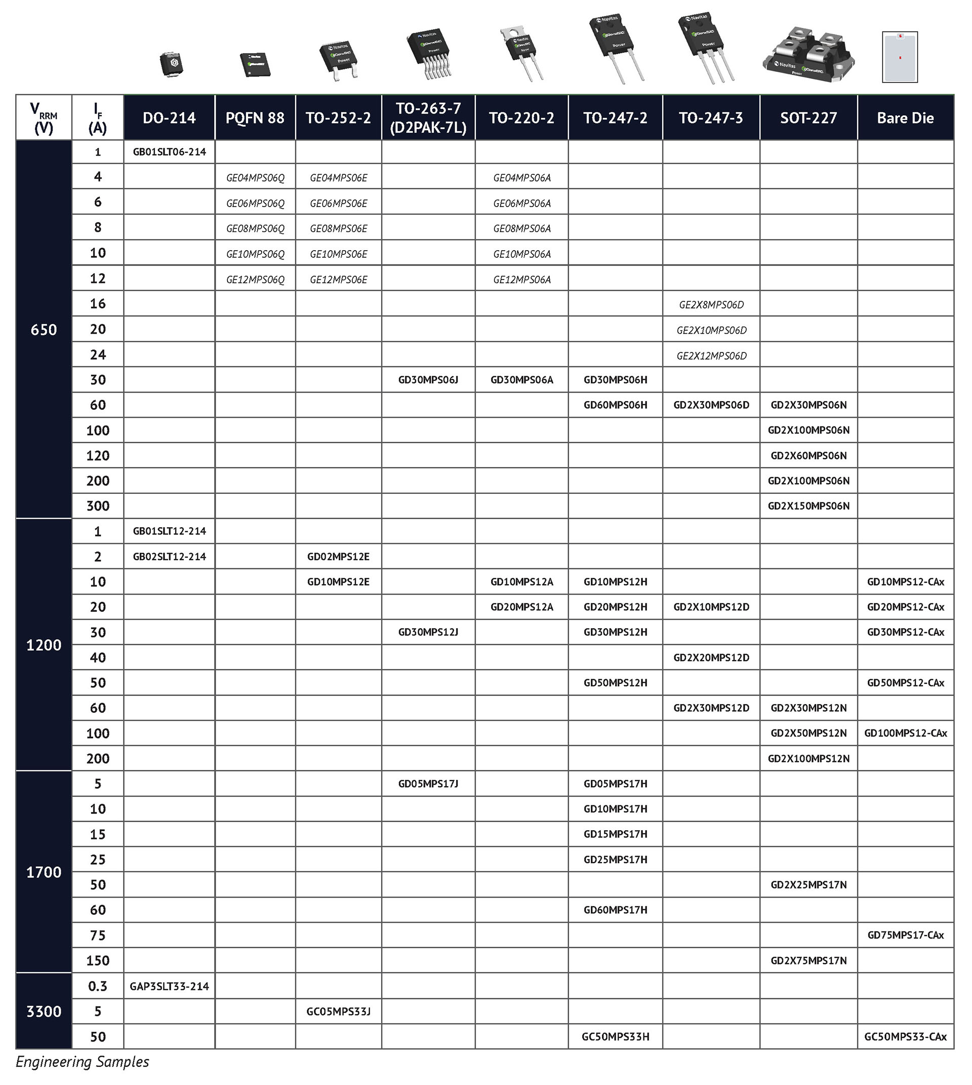
SiC Schottky MPS™ Diodes
Merged-PiN Schottky (MPS) diodes combine two beneficial features from the PIN and Schottky diode. The PIN sustains excessive surge currents with low leakage, while the Schottky element offers low forward voltage drop and fast-switching characteristics. Target applications include PFC, boost, and high-voltage, higher-power motor drives.
To access product datasheets, models, and to order parts, please click here.
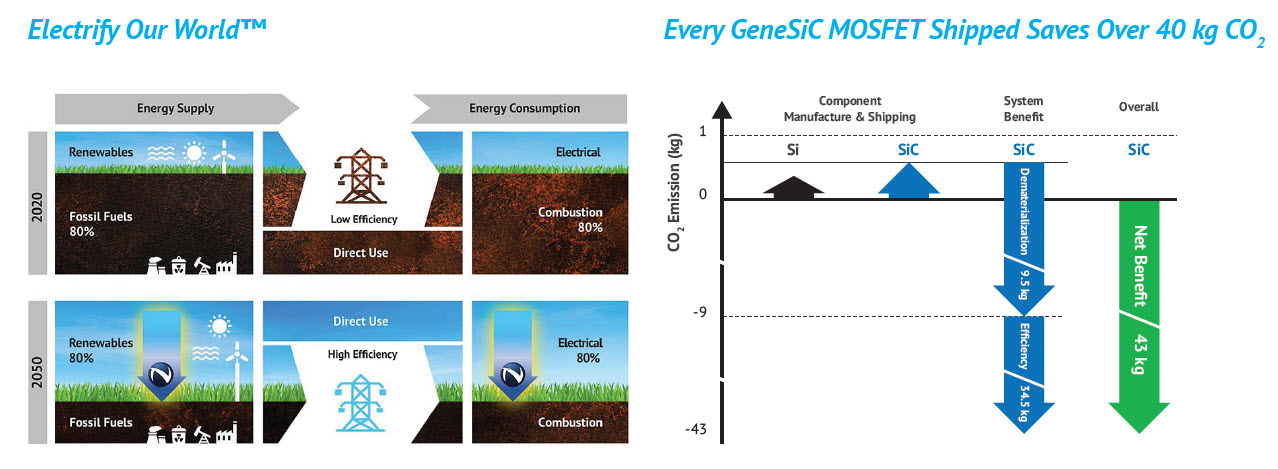
Electrify Our World™
Silicon Carbide technology enables CO2 reduction by increasing system efficiency and through ‘dematerialization’ – using less case material, heatsink, PCBs, etc. vs. legacy silicon IGBTs.
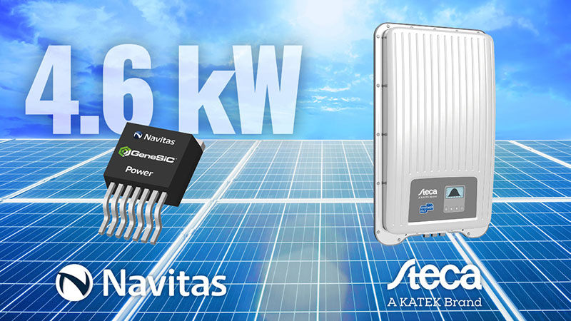
Each KATEK coolcept fleX Steca solar inverter uses 16x GeneSiC G3R75MT12J SiC MOSFETs per 4.6 kW unit. The 1,200 V, 75 mΩ-rated devices are used in a two-level converter, with bi-directional boost converters and an H4-topology for AC voltage output. Increased switching frequency shrinks the size and weight.
“Next-generation GeneSiC technology has enabled a major step in system performance without compromising our high engineering standards, especially regarding EMI,” said Dr. Peter Grabs, KATEK’s Director of Innovation, Research and Development. “Navitas’ excellent quality – with zero failures – and consistent, short lead-time delivery are critical success factors as we expand production into new markets.”
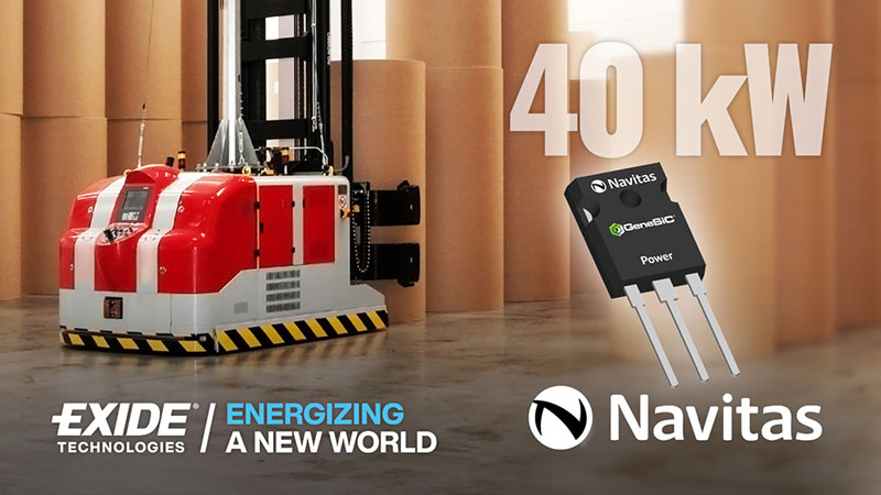
Exide’s high frequency chargers convert 220 V AC power to a battery-level voltage between 24 and 80 V for lead-acid and lithium-ion battery-powered industrial vehicles. The 7 kW module uses GeneSiC G3R60MT07D (750 V) MOSFETs and GD10MPS12A (1,200 V) MPS Schottky diodes, with frequency-optimized architecture. The same platform can be upgraded to 10 kW, with 4 modules in parallel to provide 40 kW of reliable fast-charging power.
“Exide Technologies delivers complete, carefully controlled fast-charging with close system monitoring for critical material-handling equipment, running 24/7,” said Dr. Dominik Margraf, Director Product Management Motion at Exide Technologies. “Navitas’ GeneSiC technology is easy-to-use, with excellent support, increased system efficiency, and cooler operation.”
Contact your local distributor or sales rep to discover the power of GeneSiC technology!
- Samples available immediately with short volume-production lead times
- Broadest silicon carbide portfolio – over 140 products in mass production (from 650 V to 6.5 kV)
Sales & Distribution Support
For sales / distributor listing, please click here.
Global / Online Partners
Arrow Electronics
Digi-Key Electronics
Mouser Electronics
Newark Farnell Element 14
US Partners
Richardson Electronics
NAC Semiconductor
Master Electronics
Verical
electro sonic
Contact Info
Contact Info
European Partners
Avnet Silica
Dacpol SP. Z O.O.
empa:::electronics
alfatec
TME Electronic Components
Compomill Nordic Components
Boran Technologies Ltd.
Iberica Semiconductores
Region
China
China
China
Taiwan
Korea
Korea
Japan
Japan
SE Asia
India
Asia-Pac Partners
GaNSEMI
Skynoon
Sunlord
Alltek
Melbrin
Sonion
Semisolution Supply
Chip1Stop
ExcelPoint
JP Electronic Devices
May 2024. Navitas, GeneSiC, and the Navitas logo are trademarks or registered trademarks of Navitas Semiconductor and subsidiaries.
