650V AllGaN™ Power IC for Power Supply Applications (gallium nitride)
![27_Pdf_File_Type_Adobe_logo_logos-512[1]](https://navitassemi.com/wp-content/uploads/2020/12/27_Pdf_File_Type_Adobe_logo_logos-5121.png)



650V AllGaN™ Power IC
for Power Supply Applications
4th IEEE Workshop on Wide Bandgap Power Devices and Applications (WiPDA)
Fayetteville, NC, USA. November 9th 2016.
Marco Giandalia, VP IC Design
Marco.giandalia@navitassemi
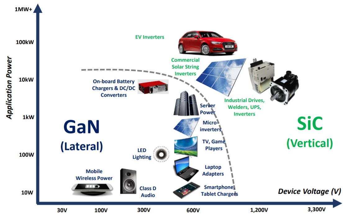
AllGaN™ applications
From GaN FET to GaN Power IC
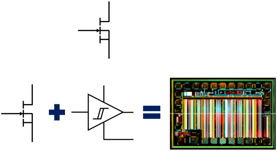
Efficient and safe gate driving
HV Monolithic GaN Power IC

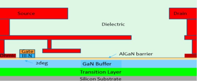
• Integration
• eMode power FET
• Optimized gate driver
• Logic and protection
• Benefits
• Reduced propagation delay
• Reduced turn-off falling time
• Reduced switching loss
• Smaller magnetics and capacitors
• Layout flexibility
Gate Driver Basic Requirements
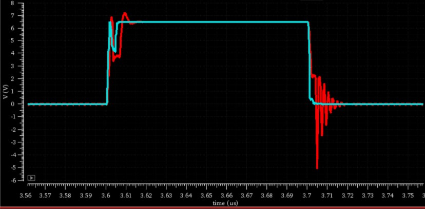
• Drive the gate with appropriate Turn-On and Turn-Off levels
• Avoid any voltage spikes or ringing that degrade the switching transition and affect device reliability
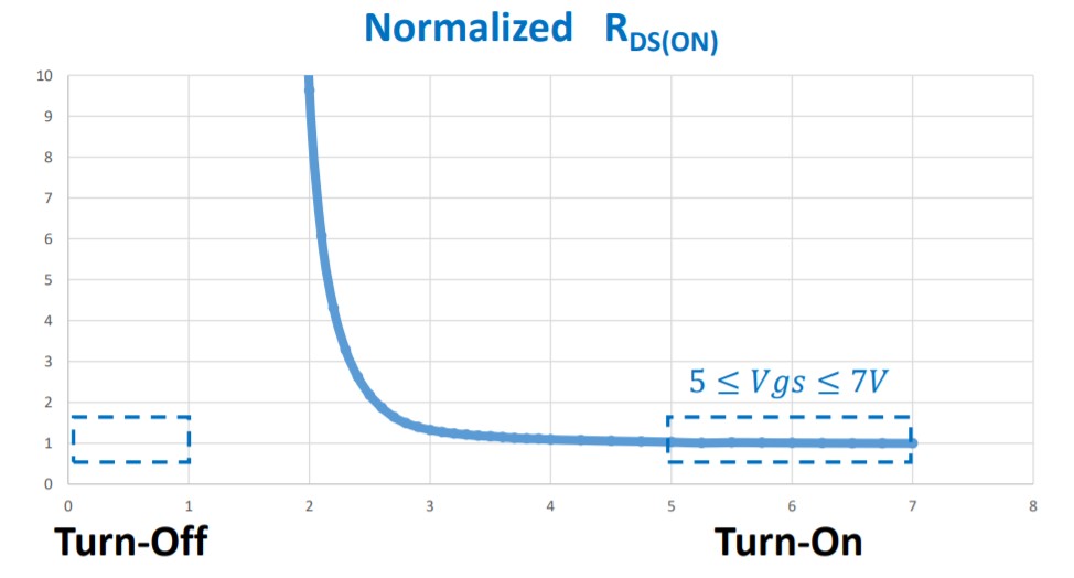
What is the Desired Voltage Range ?
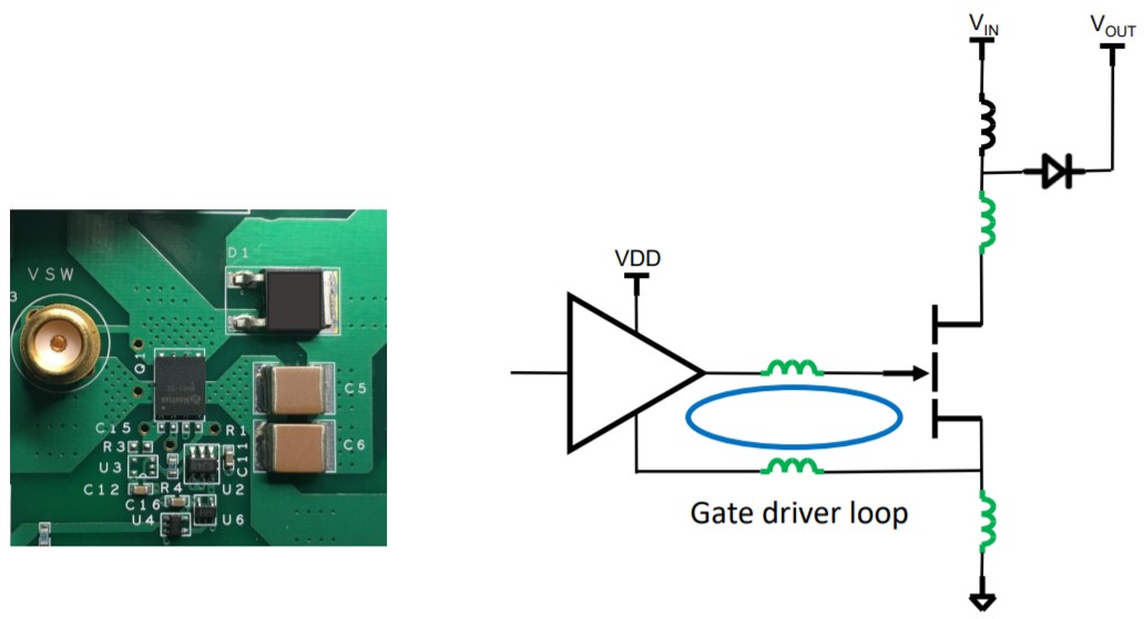
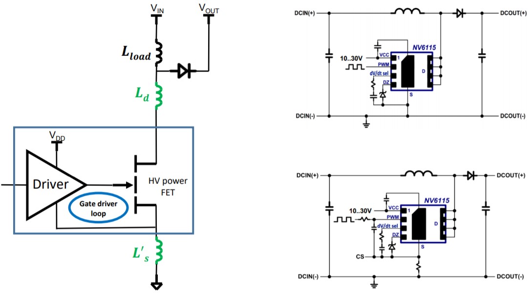
Gate Loop Equivalent Circuit:
GaN FET + External Driver
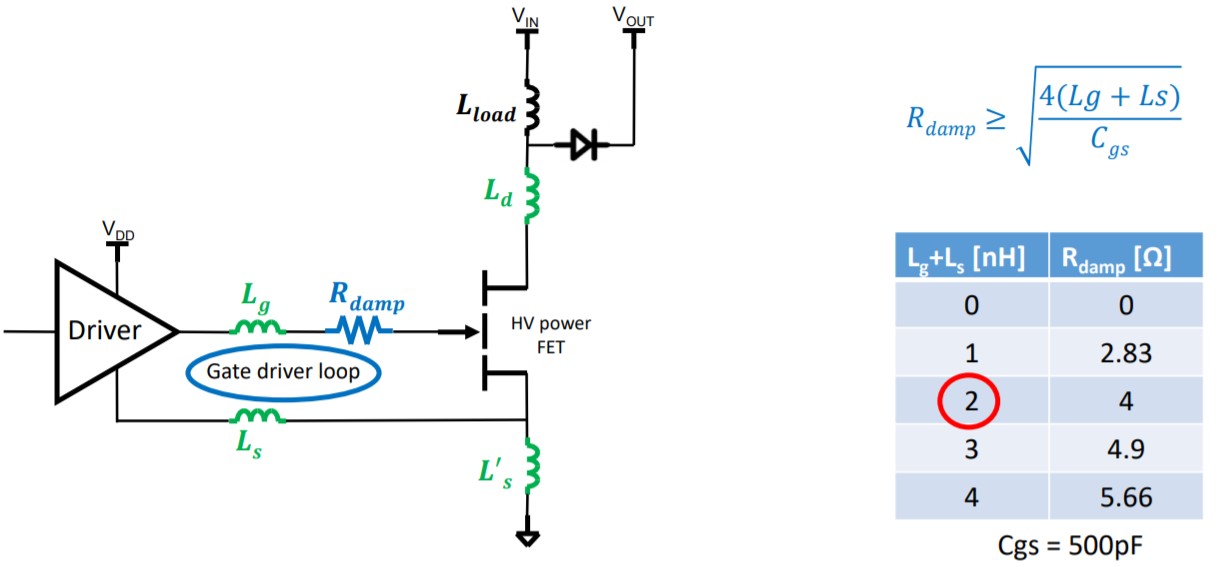
Discrete Approach Requires Rdamp
• Damping resistor is needed to reduce oscillation and voltage spike at the power FET gate
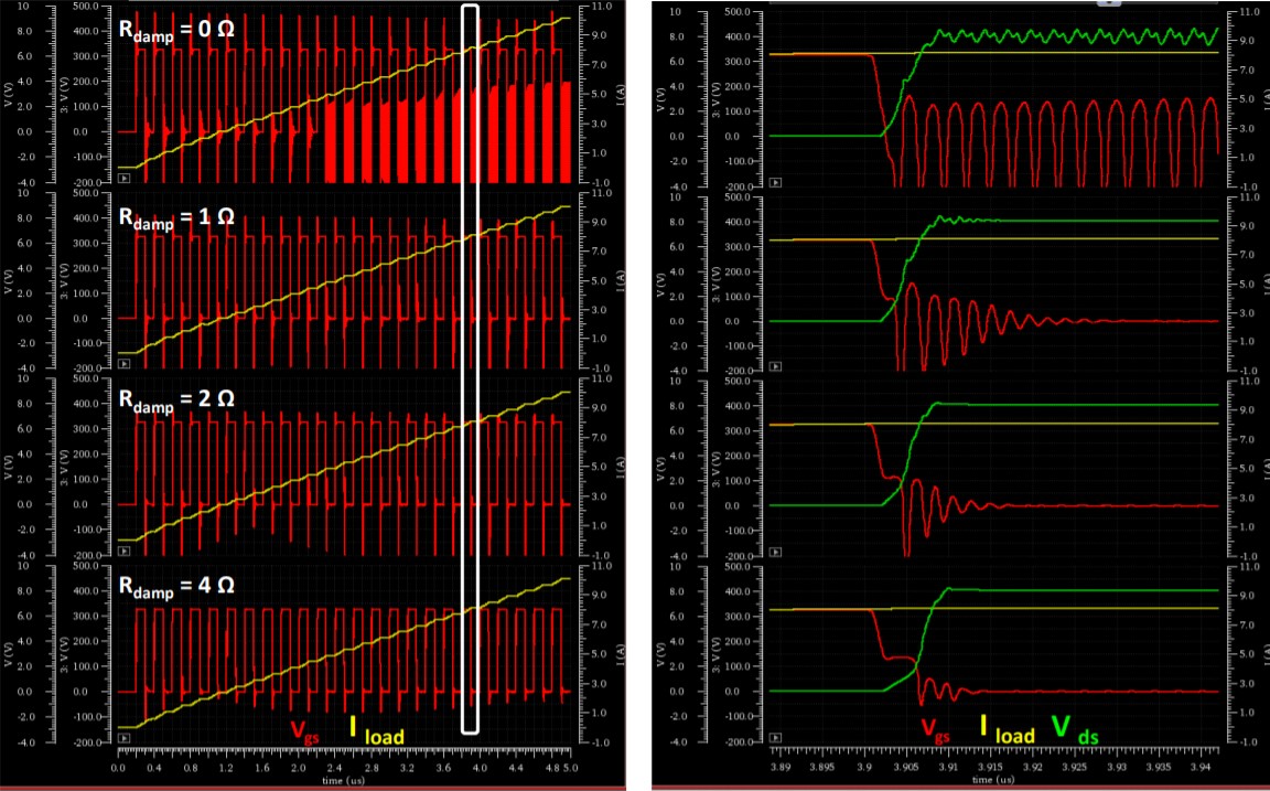
Rdamp …does?
Gate Loop Equivalent Circuit:
AllGaN™ Power IC
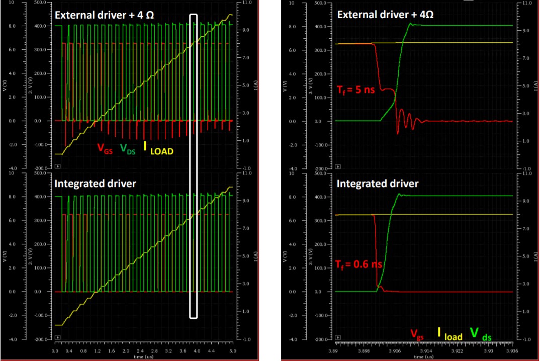
Integrated Driver: 10x faster Turn-off
Integrated Driver in ZVS
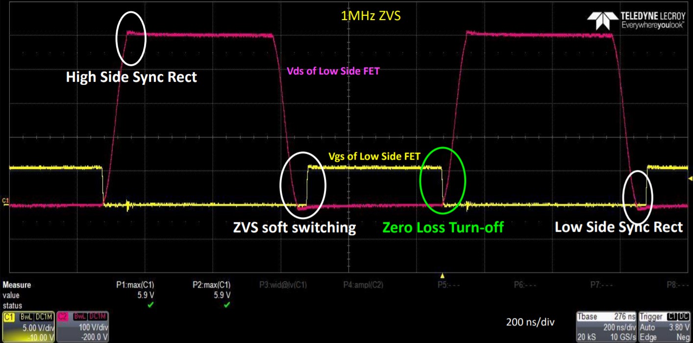
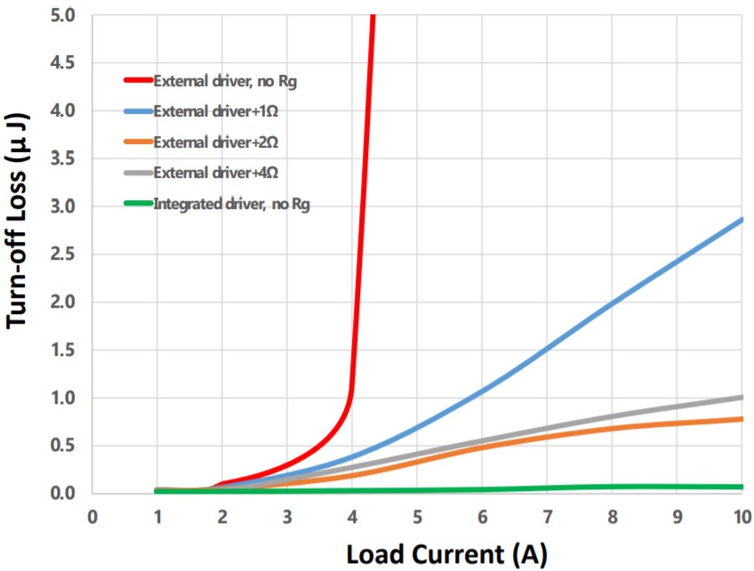
Speed & Integration → Zero Turn-off Losses
External drivers
• Significant turn-off losses
• Only few nH of gate loop
inductance causes voltage spikes
that create unintended turn-on of
the GaN FET
• Adding a gate resistor reduces
spikes but slows down the circuit
creating additional losses
Integrated GaN drivers (iDrive™)
• Eliminate the problem
• Negligible turn-off losses
Device Package
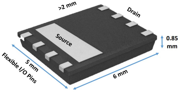
• Leadframe-based 5X6mm power package outline
• Low profile, small footprint with HV clearance
• Low inductance power connections (~0.2nH)
• Low thermal resistance (<2oC/W)
• I/O pins enough for drive functions
• Reliable
• Low cost
Device Package
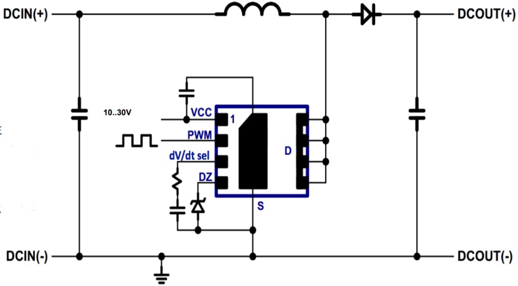
• External components:
o VCC decoupling capacitor (absolute
maximum rating 30 V)
o Zener diode as voltage reference
o RC network to set the desired turn-on
dV/dt rating (150 V/ns to 15 V/ns)
• Static Pdrv= 9 mW (only 35 mW at 1 MHz)
• Propagation delay = 10-20 ns
Half-Bridge Configuration
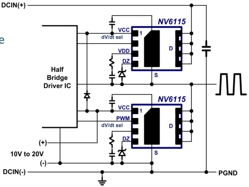
• Bootstrap circuit is the most practical and effective way to derive power supply for the high-side power FET
• When the body diode of the low side is active, the switch node goes negative by 2~4V depending on the load current amplitude
• On-chip voltage regulator ensures a stable FET gate voltage
Benchmark Power Density Today
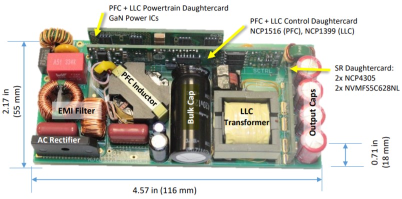
• AC-19VDC 150W (Navitas and ON Semiconductor collaboration)
• 300kHz – limited by available control ICs
• Power Density : 1.31 W/cc (21.4W/in3)
1.03 W/cc (17 W/in3) with 1.5mm case = 40% increase on best-in-class
Benchmark Power Density Today
• AC-19VDC 150W
• GaN Power ICs
• 1 MHz – DSP-controlled
• Not optimized for light-load operation
• Power Density : 26.4 W/in3 = > 2x increase vs. best-in-class


650V AllGaN™ Power IC
for Power Supply Applications
4th IEEE Workshop on Wide Bandgap Power Devices and Applications (WiPDA)
Fayetteville, NC, USA. November 9th 2016.
Marco Giandalia, VP IC Design
Marco.giandalia@navitassemi