A New 650V GaNFast Half Bridge IC for AC/DC Converter Applications (gallium nitride)
![27_Pdf_File_Type_Adobe_logo_logos-512[1]](https://navitassemi.com/wp-content/uploads/2020/12/27_Pdf_File_Type_Adobe_logo_logos-5121.png)


A New 650V GaNFast Half Bridge IC
for AC/DC Converter Applications
Santosh Sharma, Kedar Patel and Marco Giandalia
IS-1121
Outline
• Background
• GaN on Silicon
• Power ICs in GaN
• Navitas  IC platform
• Navitas Half-Bridge IC
• Why Half-Bridge IC?
• Half Bridge Architecture
• Key Features & Performance
• Navitas Half-Bridge IC
• Active Clamp Flyback (ACF) Topology
• Summary
GaN Material Properties
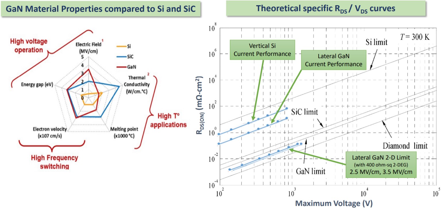
GaN Advantage for Offline Applications

• AlGaN/GaN heterojunction enables high 2DEG concentration and lateral electron mobility under channel and drift region → Low specific Rdson
• 10x higher breakdown field → High breakdown voltage
• Absence of junctions → low QG/Qoss /Qrr
• Lateral device structure → Easy to integrate different flavors of active components (eMode/dMode/Schottky) and passives with different voltage handling capabilities & good isolation
• Integration on Silicon substrate means , low cost Silicon fabs can be used
eMode vs dMode GaN
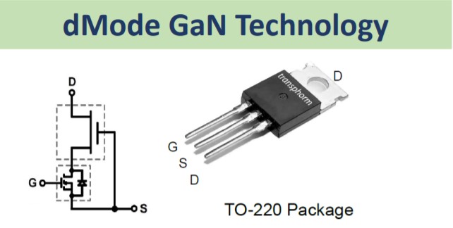
• Depletion mode GaN with Silicon FET Cascode
• Silicon FET gate easy to drive
• Complicated multi chip package
• Prone to oscillations and instability
• No dV/dt control
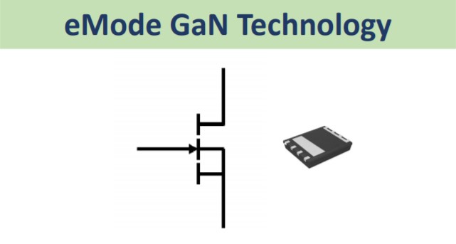
• Low QG
• Easy to package and low package inductance
• Good dv/dt control with gate access
• No reverse recovery loss
• Requires careful gate voltage control

Navitas  IC Platform

• Sets up physical and electrical constraints for IC design in GaN
• Offers great deal of design flexibility
• Fast design/tape out cycle time
• Enables seamless integration of new devices and features
• Scalable models, streamlined for voltage, process corners and temperature
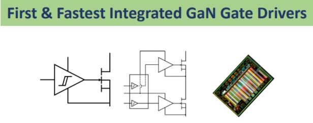

• eMode and dMode transistors
• Integrated capacitors
• Integrated resistors
• Inverters
• Buffers
• Logic gates
• Pulse generators
• ESD I/O circuits
• Hysteretic Digital input
• Wide operating power supply range (10V – 30V)
• Regulated internal power supply
• Integrated Bootstrap
• Integrated level shifters
• Protection:
• UVLO
• ESD
• Shoot-through
• Monolithic GaN integration
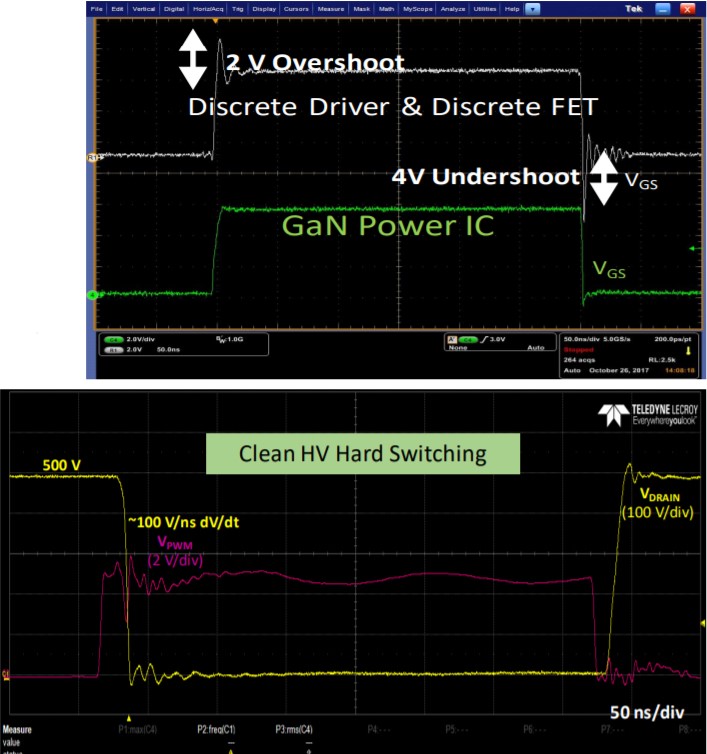
Navitas Integrated Drive Solution
Driver challenges addressed by Navitas power ICs:
• Eliminates gate voltage oscillations
• Excellent Miller immunity (>150V/ns)
• Well regulated gate drive voltage
• Extremely low turn off losses
• Gate ESD protection
• Externally programmable dv/dt control for EMI/noise reduction
• Extremely fast turn on and turn off speeds (<5ns)
• Clean HV switching characteristics
• Fast chip startup capability
• Low standby power losses
• Safe power up and power down
• Low cost/low PCB real estate and PCB layout insensitive
Half-Bridge Level-Shifter Options

Conventional Si JI based level shifters
• High junction capacitances
• Very Lossy
• Unsuitable for high frequency
switching applications
High Frequency Isolators
• Capacitive and Inductive coupled isolators
• Multiple die structures using capacitor plates or magnetic coils
• Use disparate materials
• Low power consumption but very costly fabrication and assembly process
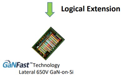
Fully Integrated Half Bridge Drivers
• Leverages low RDS/QG/COSS & high VDS GaN for HV level shifting
• Level shifters can be made extremely small and fast
• Very low current resulting in low power loss
• High common mode noise immunity
• Pulsed level shifting
 Half-Bridge GaN Power IC

• Combination of extremely fast low-power consumptive level shifters, Zero QRR/low RDS bootstrap FET, integrated gate drive + power stage enables multi MHz operation with short propagation delays and low system losses!!!
• Integrating drivers, level-shifters, bootstrap FET and power FETs in a monolithic package reduces PCB footprint
 Half-Bridge GaN Power IC
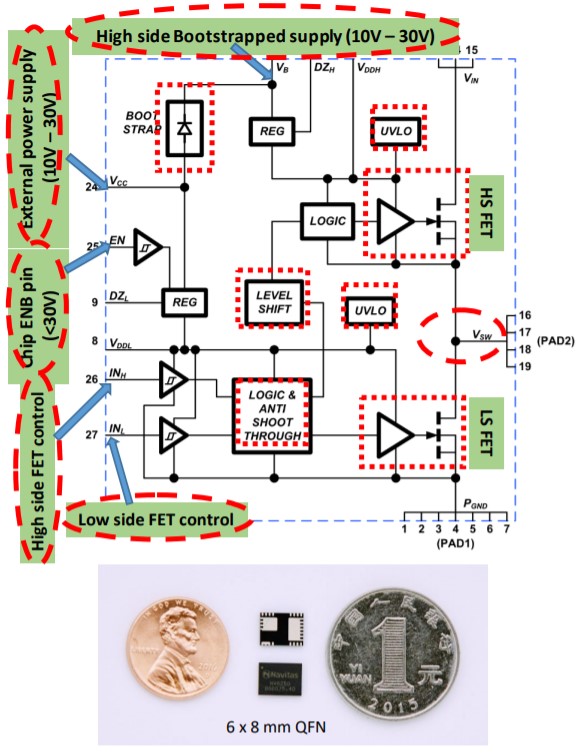
• 2x GaN FETs (High side and Low side) & 2x GaN drivers
• Gate voltage regulation
• Hysteretic digital inputs
• Compatible with a wide range of analog and digital controllers
• Integrated high voltage bootstrap FET for fast bootstrap capacitor charging capable of high frequency operation
• Level-shift circuit; low loss/fast and >200V/ns CM noise immunity
• UVLO for safe startup and shut down
• ESD protection
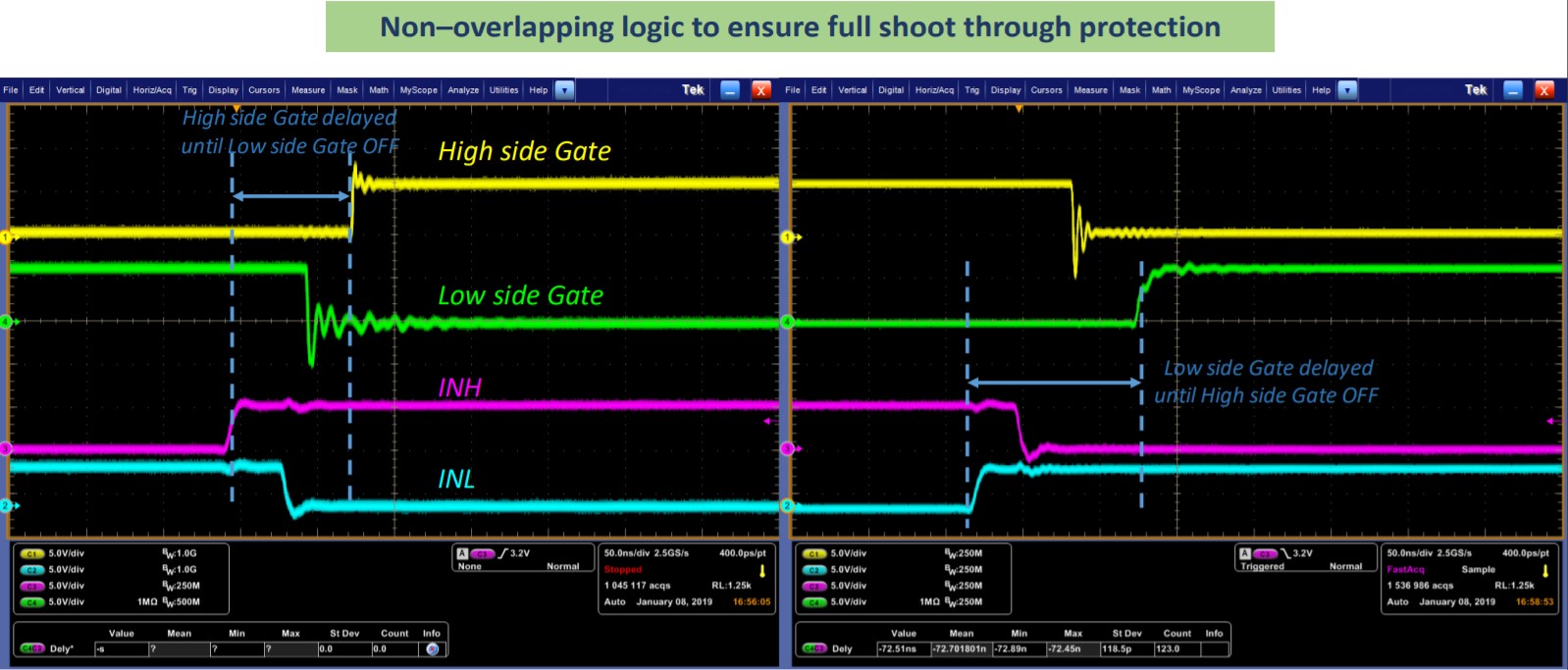
• Shoot-through protection (non overlapping logic)
• Chip enable function for low loss standby mode operation
Half-Bridge Startup
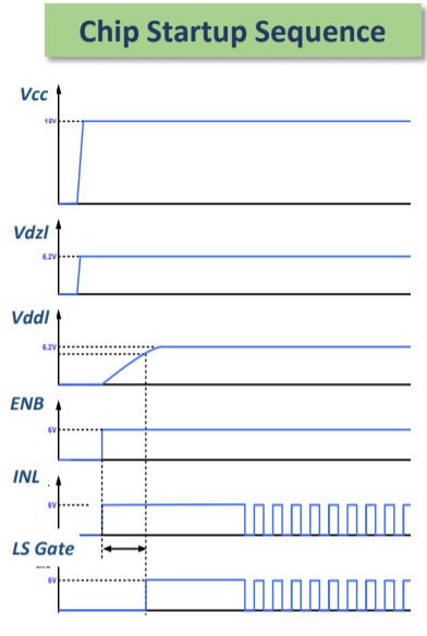
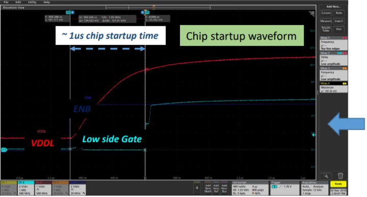
1. ENB = 0V chip kept in “Standby”
• This shuts of the internal regulator
• <190uA current draw from VCC @ 15V
2. ENB = HI; Internal regulator will turn on and start charging VDDL
3. Low side chip comes out UVLO
4. Low side gate switches in response to INL signal
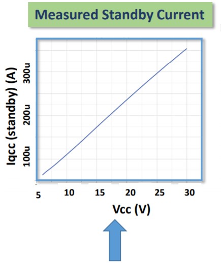
• Very low standby PLOSS (<10mW)
• Fast startup coming out of
standby mode
Half-Bridge Performance
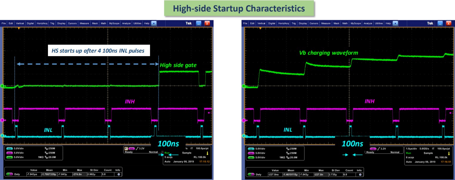
• Integrated bootstrap FET charges the high side power supply when INL = HI
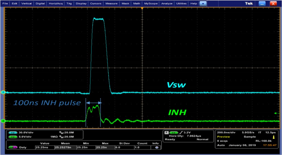
• Chip capable of fast charging high side bootstrapped power supply even for INL pulses as small as 100ns
• Bootstrap FET immune to dv/dt induced noise – clean high side power supply charging profile
• Ideal for high frequency operation
Half-Bridge Performance
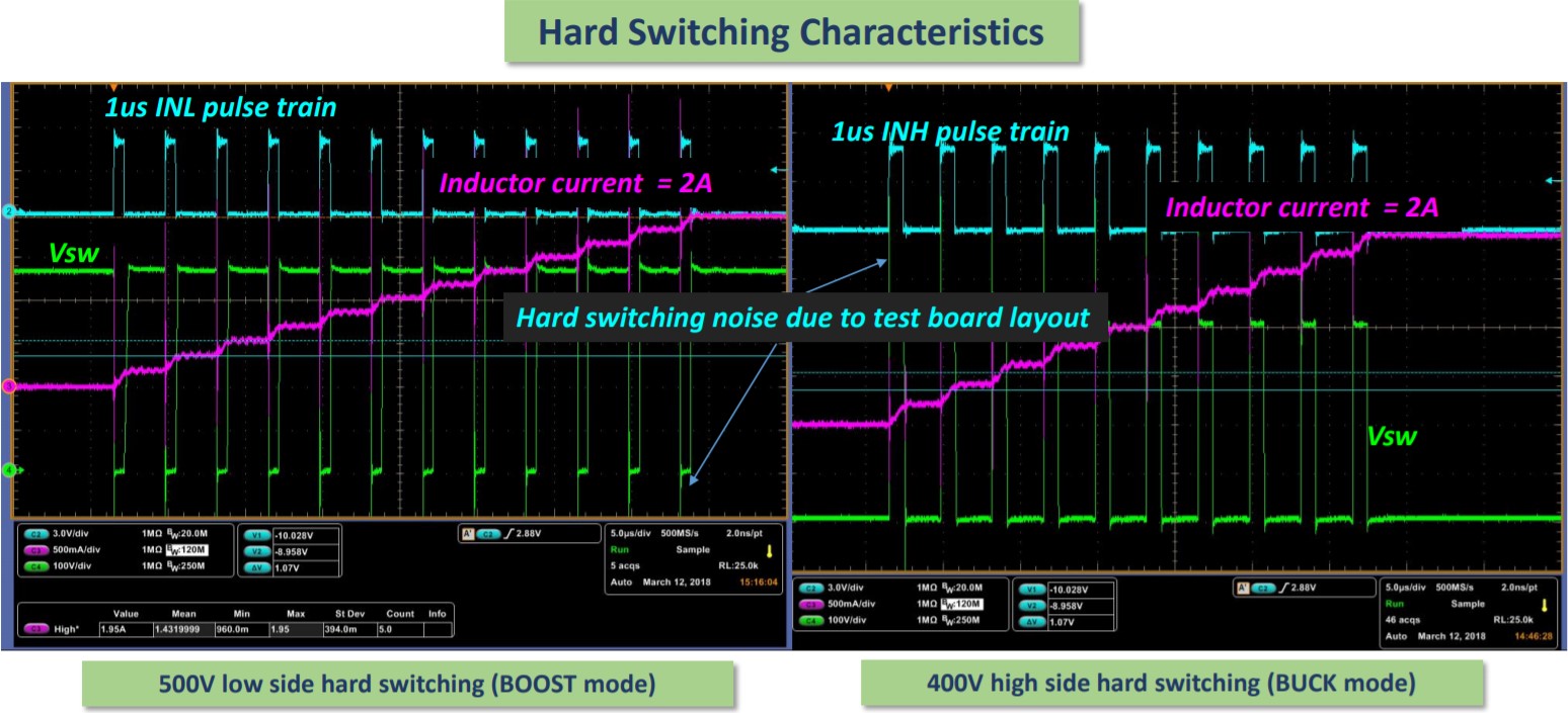
Excellent common mode noise immunity – chip can handle very stressful hard switching environments
Half-Bridge Performance

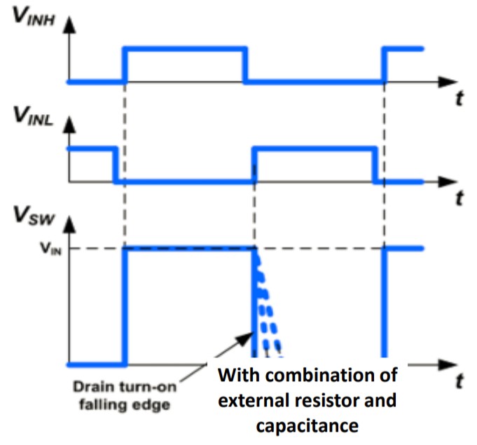
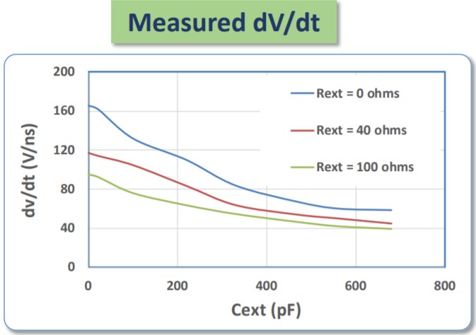
• Ability to modulate hard switched edge dv/dt important to reduce system noise and reduce EMI
• Low side FET dv/dt can be modulated by adding external components
Half-Bridge Performance
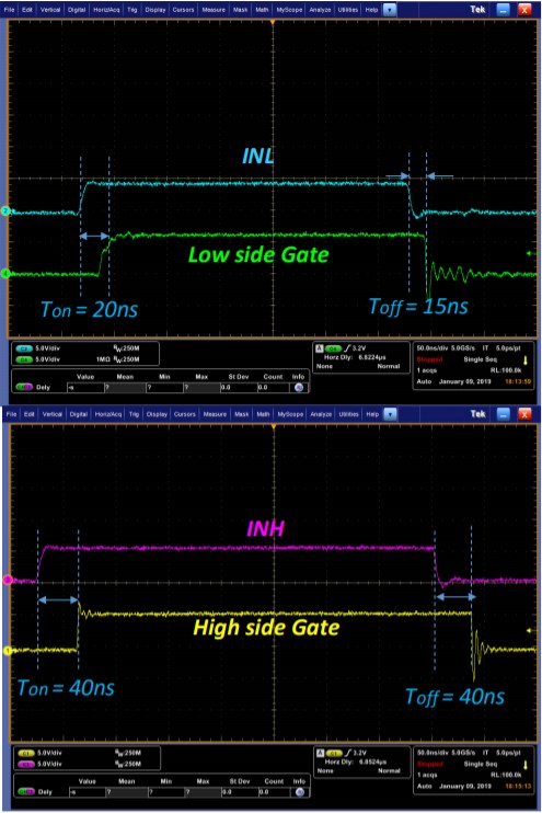
• Typical propagation delays
• Low side: TON = 20ns , TOFF = 15ns
• High side: TON = 40ns, TOFF = 40ns
• Chip capable of transmitting 100ns high side pulses even under hard switching conditions
Half-Bridge Performance
Half-Bridge Performance
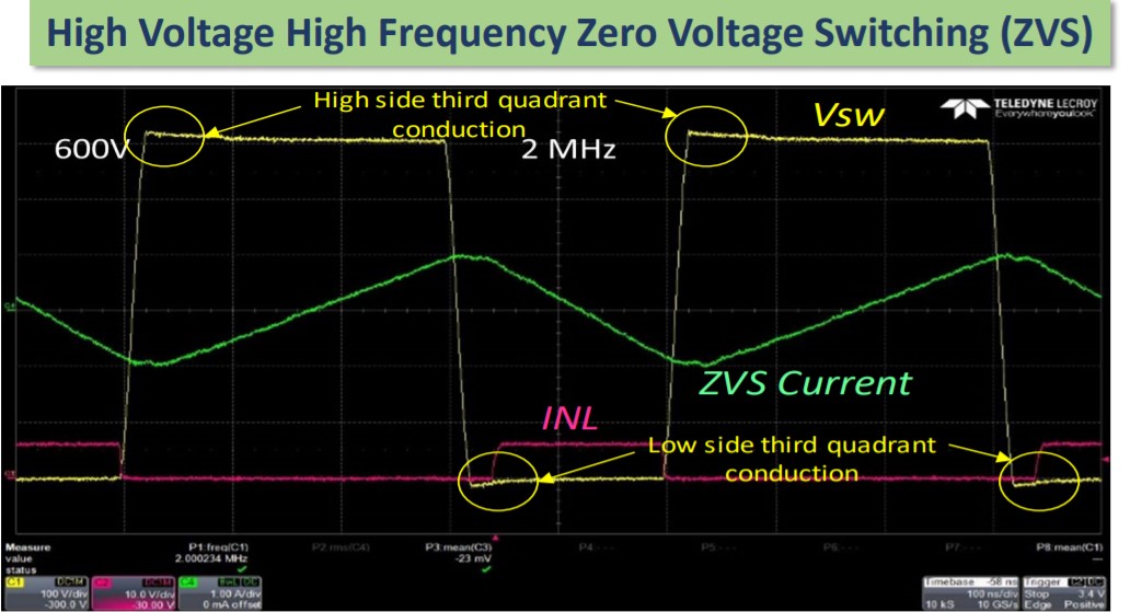
What makes the half bridge IC ideal for high frequency ZVS applications?
• Low COSS of power FETs
• Low TON and TOFF
• Ability to transmit ON pulses during dv/dt
• High dv/dt immunity (no false ON or OFF pulses due to dv/dt induced noise)
Half-Bridge Performance
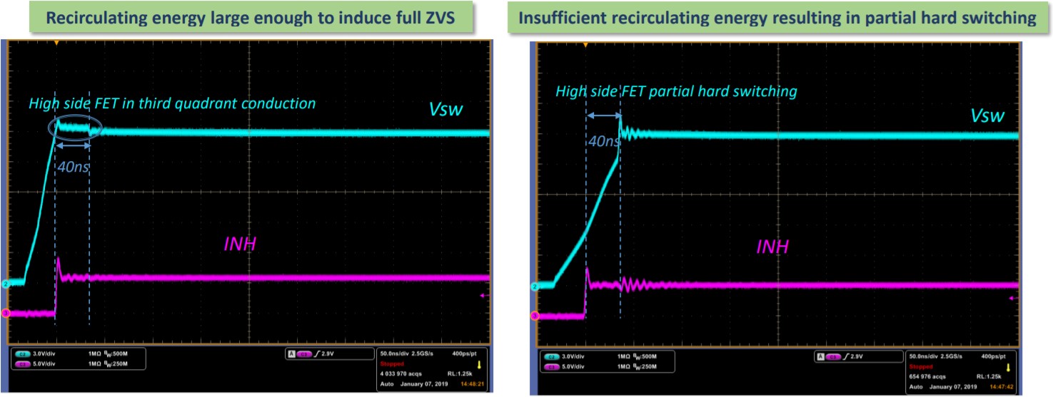
• Level shifter capable of transmitting ON pulses over a wide range of VSW dv/dt’s without any degradation of turn on prop delay
• Critical attribute of the half bridge IC – specially under light load or startup conditions which demand some partial hard switching capability
Active Clamp Flyback (ACF) Topology
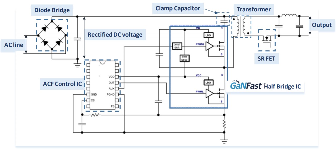
• ACF is an advancement over the standard hard switching Quasi-Resonant (QR) Flyback Converter
• Adding an extra switch (high side of the Half Bridge IC) enables ZVS
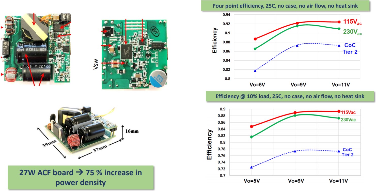
• Reduces switching loss and enables frequency increase -> minimize transformer/EMI filters size and cost
• Increase power density and efficiency!!!
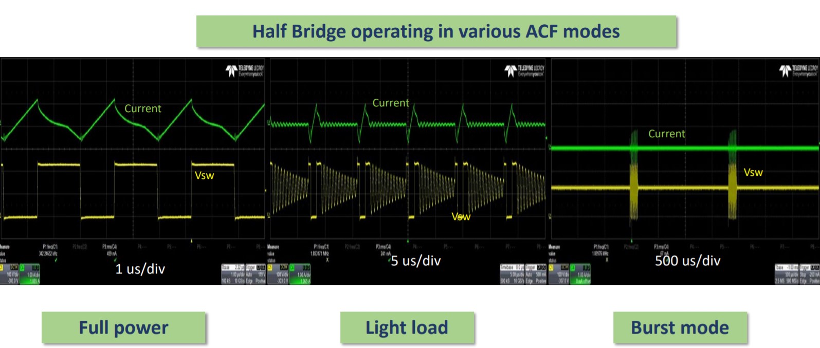
Half Bridge IC in ACF
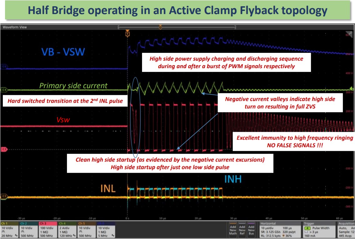
Half Bridge IC in ACF
27W USB PD Charger
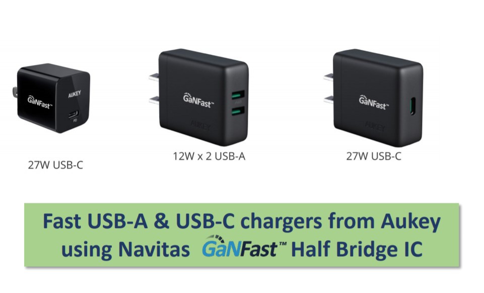
Mobile Charger Application
Summary
• Innovative Half-Bridge GaN power IC developed using Navitas
proprietary GaN-on-Si technology and PDK
• Sets a new paradigm in efficiency and power density for AC/DC power conversion
• Ideally suited for ACF topology that is commonly employed in
consumer adapter solutions over a wide range of power from
10W – 100W
