Active Clamp Flyback Using GaN Power IC for Power Adapter Applications
![27_Pdf_File_Type_Adobe_logo_logos-512[1]](https://navitassemi.com/wp-content/uploads/2020/12/27_Pdf_File_Type_Adobe_logo_logos-5121.png)


Active Clamp Flyback Using GaN Power IC for
Power Adapter Applications
Linqxiao (Lincoln) Xue, Staff Applications Engineer, [email protected]
Jason Zhang, VP Applications, [email protected]
March 29th 2017
How to Improve Power Adapter Density?
Traditional Travel Adapter and Chargers
USB PD and Quick Charge

• Added power in USB PD and Quick Charge requires dramatically higher power density (>20 W/in3)
• Higher efficiency and lower power loss are required in high density adapters
• How to dramatically improve the power density?
Outline
• Added power in USB PD and Quick Charge requires dramatically higher power density (>20 W/in3)
• Higher efficiency and lower power loss are required in high density adapters
• How to dramatically improve the power density?
QR Flyback Hits Performance Ceiling

• Frequency-dependent losses
• Leakage inductance loss
• Snubber/clamp losses
• Partial hard-switching loss at high line
• Slow turn-on loss to minimize EMI
• Difficult to improve efficiency at high frequency
ACF Enables ZVS and High Frequency Switching

• No snubber losses, all leakage energy is recovered
• ZVS soft switching over entire operation range
• ZCS soft turn-off for output rectifier
• Clean waveforms reduce EMI
• Enable small adapter design with high-frequency switching
ACF Operation
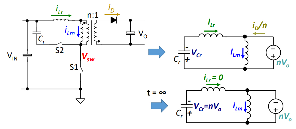
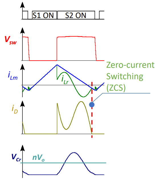
• Lr resonates with Cr during S2 ON interval
• ZVS is achieved by magnetizing inductance current
• Rectifier current is the difference between iLm and iLr
• iLr returns to iLm by the end of S2 ON interval for rectifier ZCS
Drawbacks of Traditional ACF


• Difficult to shape the current to achieve ZCS and minimize rms current
• Conduction loss is high
• Not compatible with SR controllers
New ACF Using Secondary Resonance
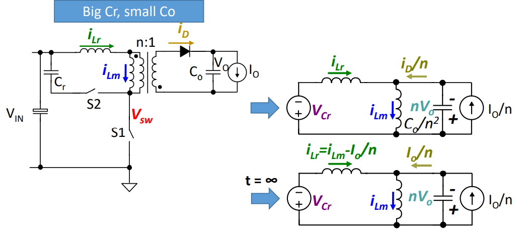
• S1 ON interval is the same as primary resonant
• In S2 ON interval
• Co/n2 << Cr , Co resonates with Lr
• iLr centers around a line lower but in parallel with iLm
• ZCS is easily achieved. No rectifier current double dipping
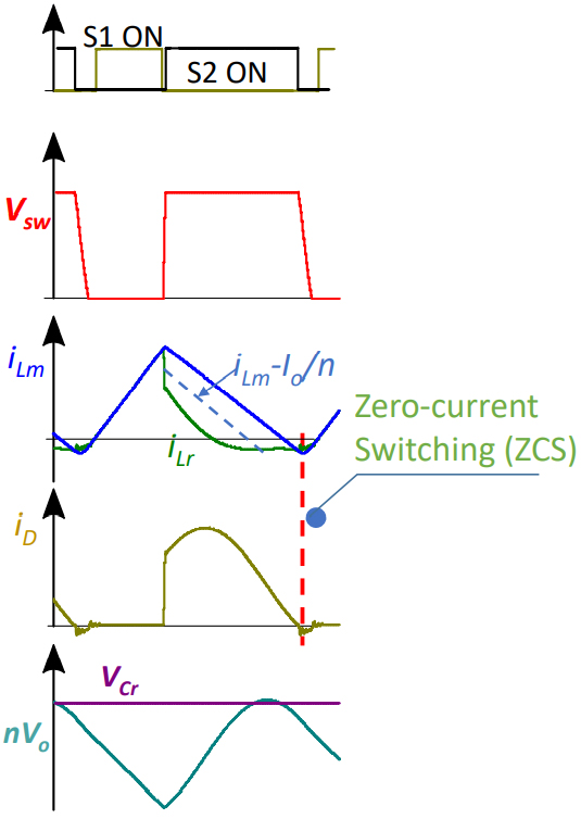
New ACF Simplifies SR and Reduces Current RMS
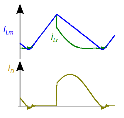

• iLr current can be easily shaped
• No rectifier current dipping issue. Simplifies SR
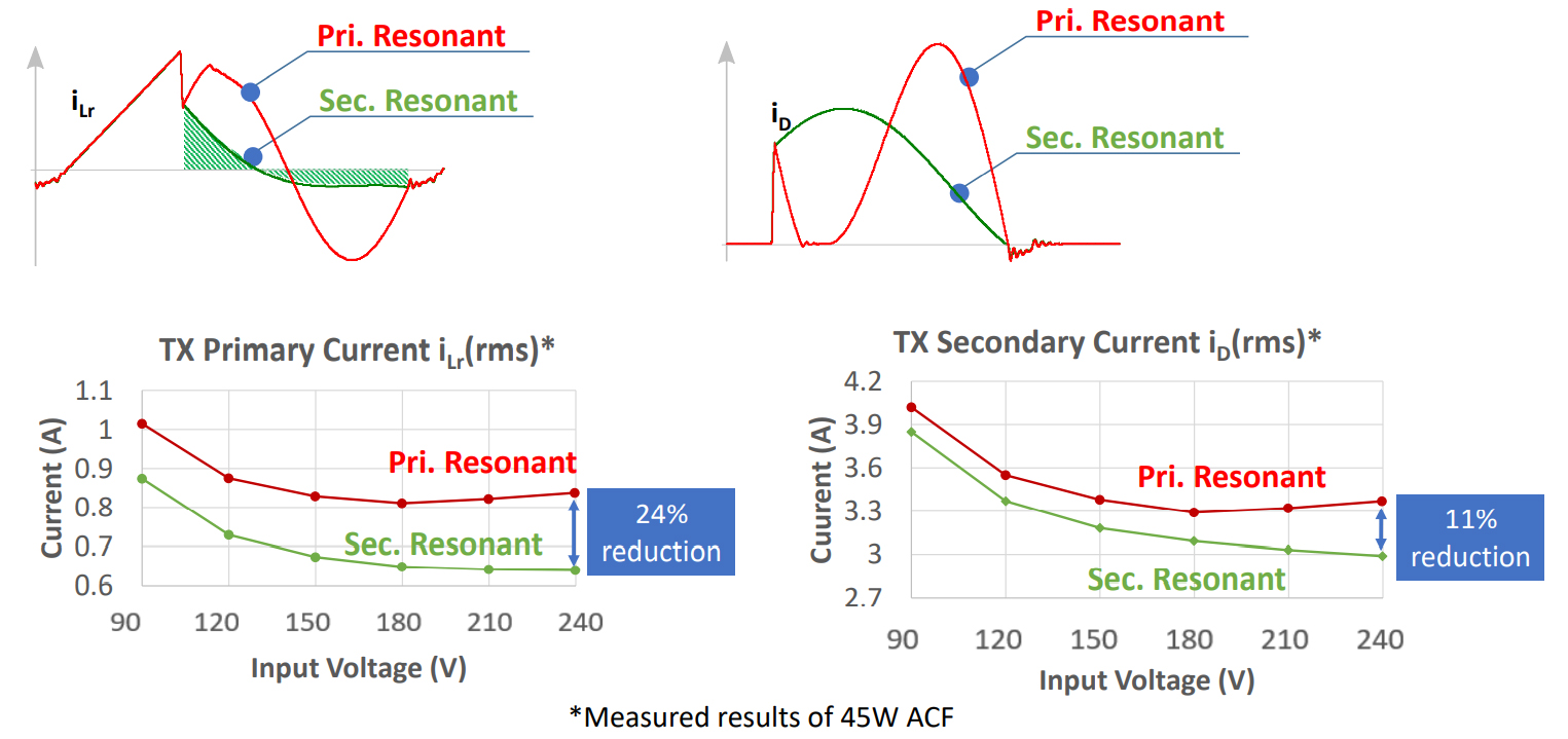
• Reduced rms current and conduction loss
Experimental Result of RMS Reduction
Efficiency Benefit of New ACF
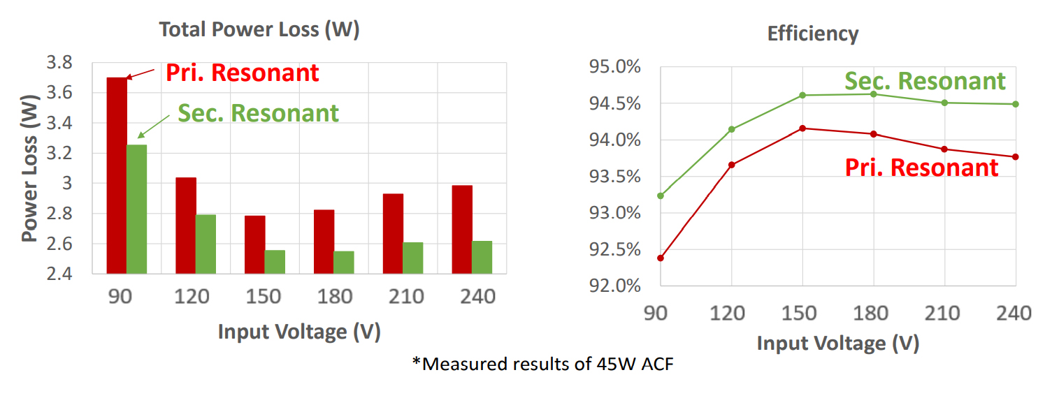
• 0.4 W power loss reduction
• ~0.8% efficiency improvement
Advantages of Using GaN in ACF
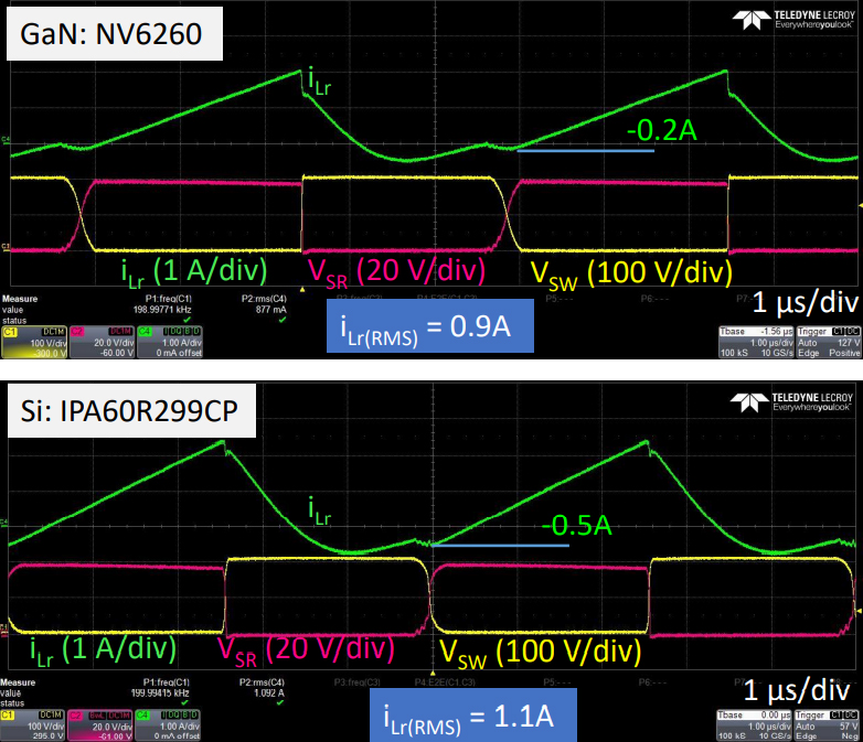
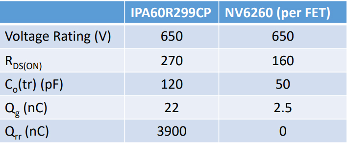
• GaN ACF needs only 0.2A negative current for ZVS vs. Si’s 0.5A
• GaN ACF RMS is only 0.9A vs. Si’s 1.1A
• GaN has no body diode loss
• Low high-frequency gate-charge loss
Half-Bridge iDrive GaN Power IC
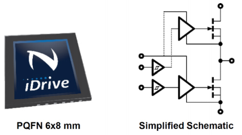
• Internal level-shift, bootstrap
• Range from 150-600 mOhm (650V)
• Single component
• Ground-referenced PWM signals
• Active Clamp Flyback, Half-Bridge, LLC, etc.
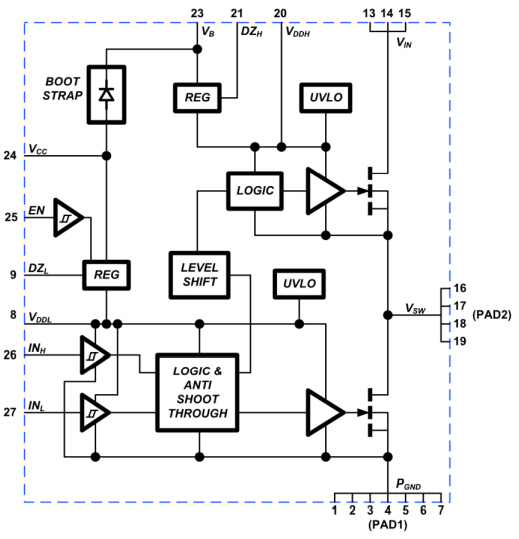
GaN Power IC Simplifies ACF
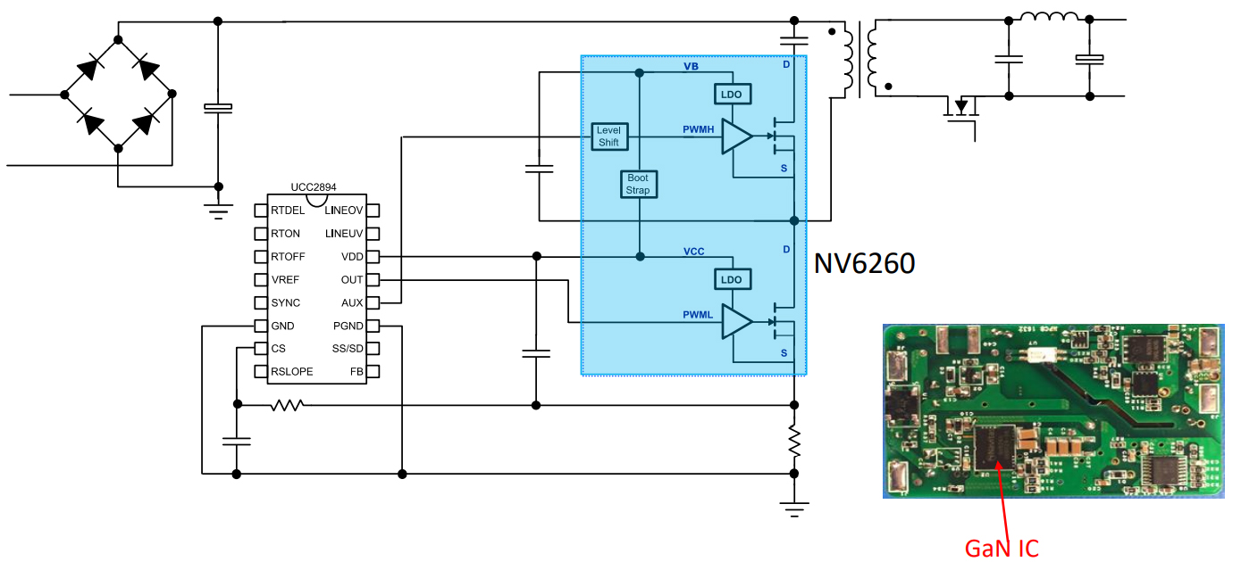
GaN Power IC Efficiency Advantage
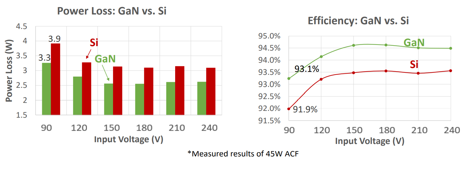
• GaN reduces power loss by 0.6W
• GaN boosts efficiency by 1.2%
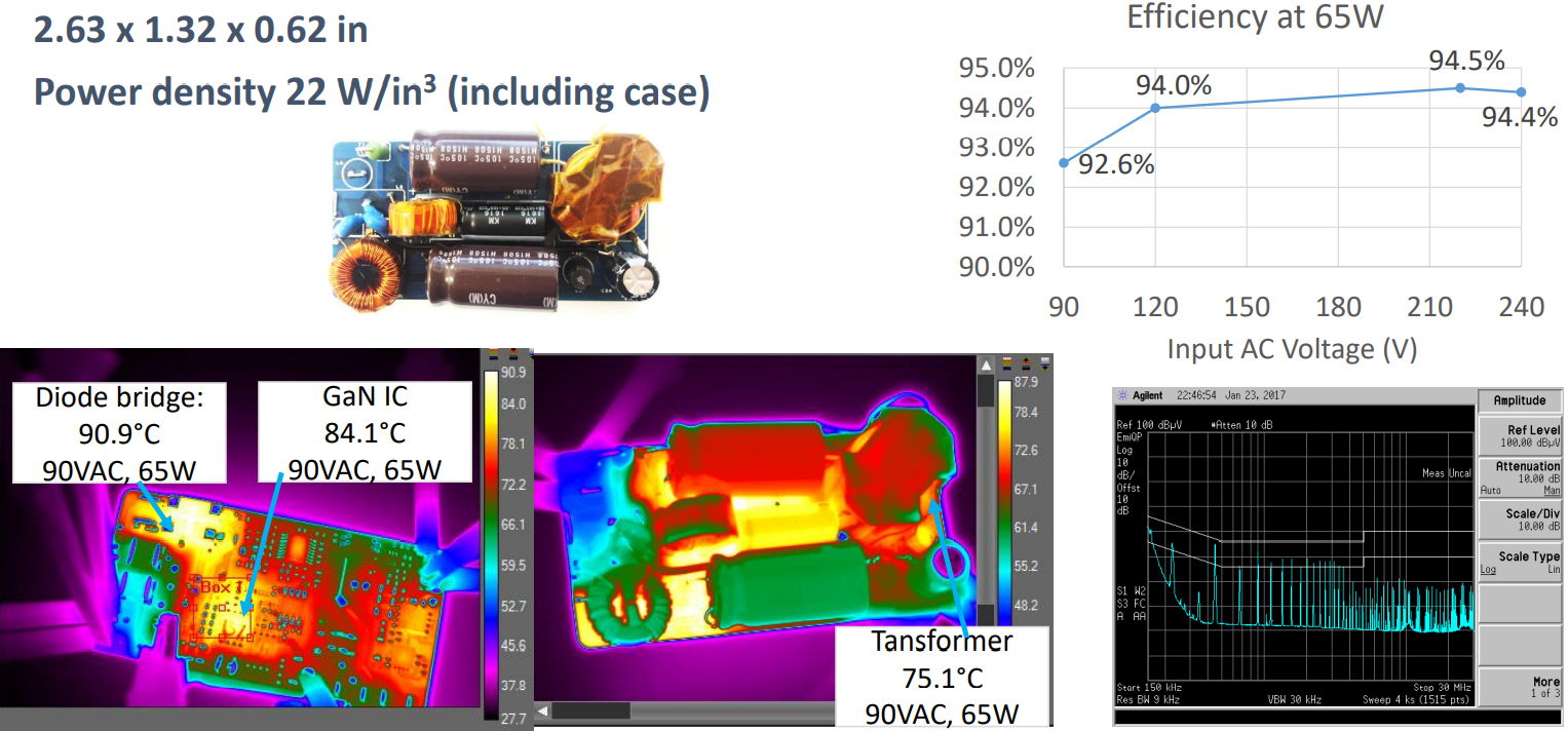
High Density 65W Adapter Using ACF and GaN
Conclusion
• USB-PD and QC demand high density solutions
• QR flyback hits performance ceiling
• ACF overcomes QR limitations and enables high frequency operation
• New ACF using secondary resonance improves ACF’s operation and
efficiency
• GaN is uniquely suitable for high frequency operation
• Half-Bridge GaN Power IC simplifies ACF design and improves density
• An example of 65W ACF adapter using GaN and secondary resonance
achieves 22W/in3 density, while meeting thermal and EMI requirement
Benchmark Power Density Today
• AC-19VDC 150W
• GaN Power ICs
• 1 MHz – DSP-controlled
• Not optimized for light-load operation
• Power Density : 26.4 W/in3 = > 2x increase vs. best-in-class




650V AllGaN™ Power IC
for Power Supply Applications
4th IEEE Workshop on Wide Bandgap Power Devices and Applications (WiPDA)
Fayetteville, NC, USA. November 9th 2016.
Marco Giandalia, VP IC Design
Marco.giandalia@navitassemi