AN010: Thermal Management of GaNFast™ Power ICs
![27_Pdf_File_Type_Adobe_logo_logos-512[1]](https://navitassemi.com/wp-content/uploads/2020/12/27_Pdf_File_Type_Adobe_logo_logos-5121.png)

Application Note AN010
Thermal Management of GaNFast™ Power ICs
Introduction
Overview
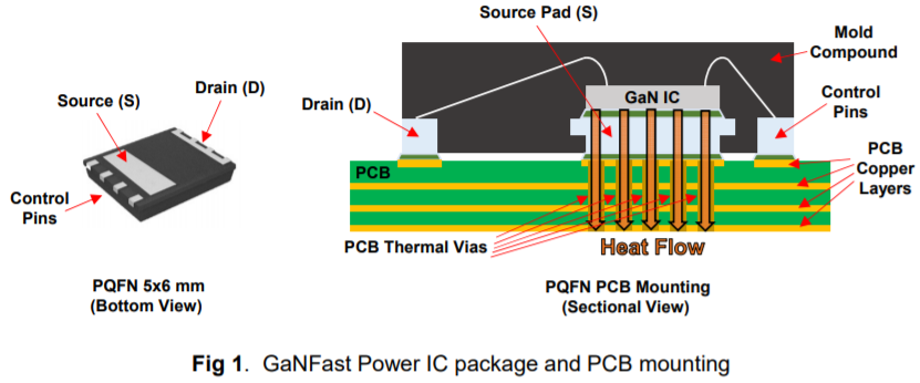
Navitas GaNFast Power ICs are available in a 5×6 mm PQFN package. The IC pinout includes a Drain pad (D), a Source pad (S), and 4 control pins. The control pins manage the gate drive supply and on/off control of the GaN power FET, and the switching currents of the external power conversion circuit flow from the Drain pad to the Source pad during each on-time period. The IC is mounted internally on the Source pad and then over-molded with plastic molding compound. All of
the exposed package pads and pins on the bottom side of the package are then soldered down to the PCB. Since the IC is mounted directly on the Source pad (S), the heat from the GaNFast IC must be taken out through the bottom of the GaNFast IC, to the Source pad (S), and through the solder to the PCB board. Thermal vias are then used to transfer the heat to the opposite side of the PCB where it can then be cooled.
Revised 3-13-19

Page 1

Application Note AN010
PCB Guidelines
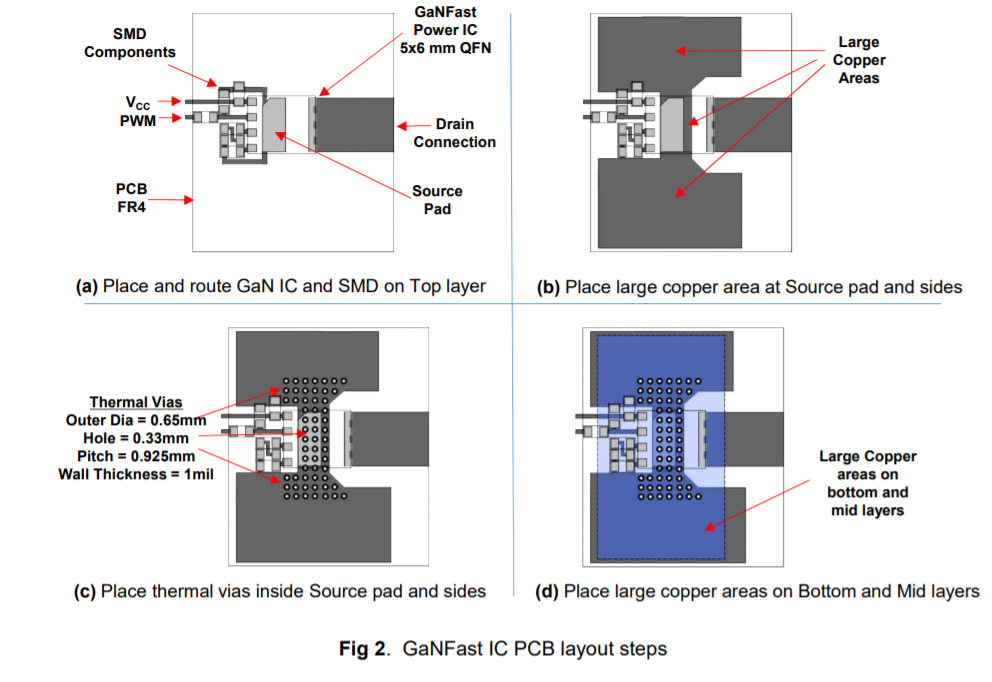
When designing the PCB layout for the GaNFast Power ICs, several guidelines must be followed in order to achieve acceptable device temperatures. Thermal vias must be used to conduct the heat from the top layer IC Source landing pad to the bottom layer and large copper areas are used for PCB heatsinking. The following layout steps and instructions illustrate best layout practices for optimal IC thermal performance.
1) Place the GaNFast IC 5×6 mm PQFN footprint on the PCB top layer.
2) Place the additional SMD components required for the control pins on the top layer (CVCC, CVDD, RDD, DZ). Place the SMD components as close as possible to the IC pins!
3) Route the connections for the SMD components, control pins, and Drain and Source pad all on the top layer.
4) Place large copper areas on the top layer at both sides and connecting to the Source pad.
5) Place thermal vias inside the Source pad and at both sides of the Source pad.
6) Place large copper areas on all other layers (bottom, mid1, mid2).
Revised 3-13-19

Page 2

Application Note AN010
PCB Layout Example (Single Low-side Switch Configuration)
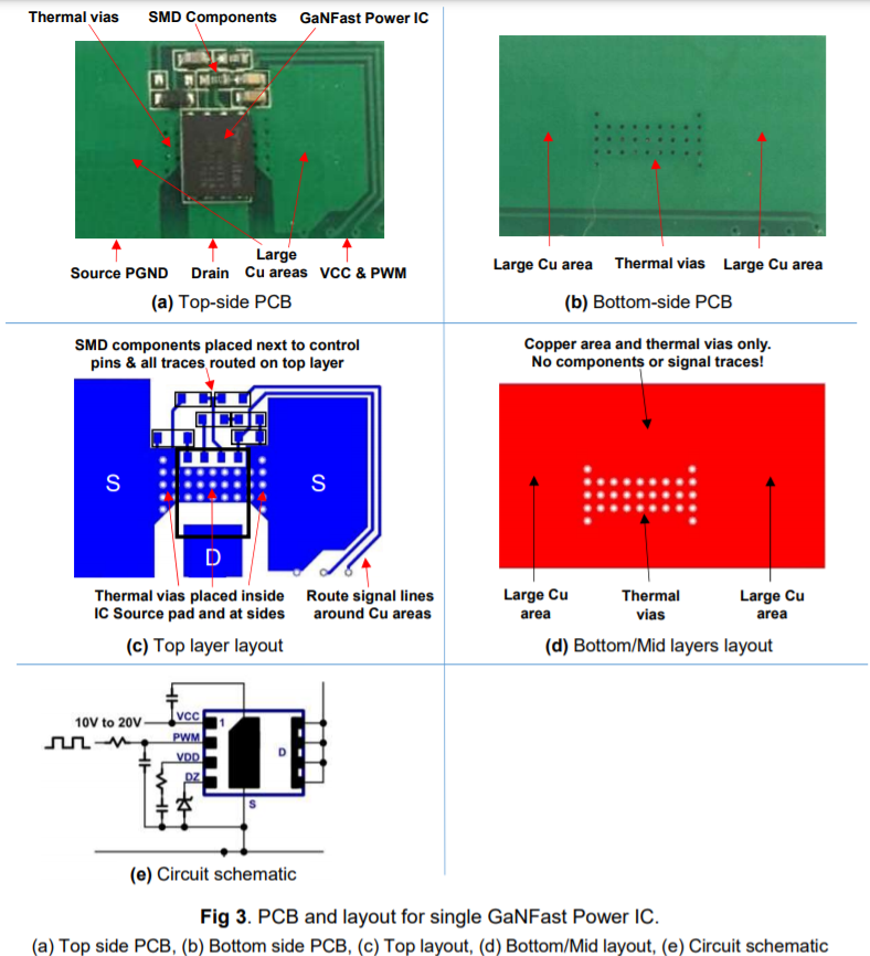
The following example (Figure 3) shows correct layout practices implemented on actual power supply PCB designs. Components and traces are all on top layer. Bottom and mid layers are for copper areas and thermal vias only
Revised 3-13-19

Page 3

Application Note AN010
PCB Layout Example (Half-Bridge Configuration)
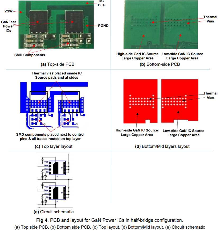
The following example (Figure 4) shows correct layout practices for half-bridge configuration. All components and connections are realized on top layer allowing all other layers to be used only for copper area and thermal vias.
Revised 3-13-19

Page 4

Application Note AN010
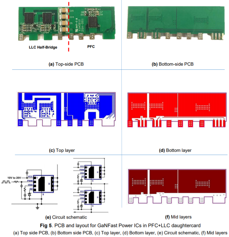
PCB Layout Example (PFC and LLC GaN daughtercard)
The following example (Figure 5) show correct layout practices implemented on actual power supply designs
Revised 3-13-19

Page 5

Application Note AN010
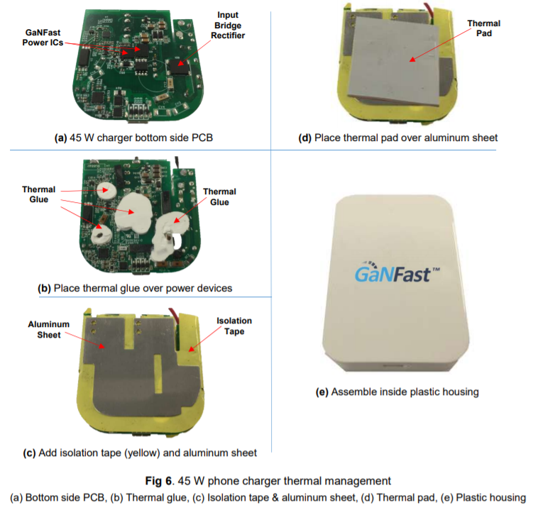
Thermal Management with Case (45 W Charger example)
When placing the power supply PCB board into a housing, additional thermal management is required to properly conduct the heat from the PCB to the case. This is necessary to avoid high component temperatures and reduced efficiency. The following 45W phone charger example (Figure 6) uses thermal glue placed on top of the power components, followed by isolation tape and an aluminum sheet for heat spreading. A thermal pad is then used to conduct the heat from aluminum sheet to the plastic case.
Revised 3-13-19

Page 6

Application Note AN010
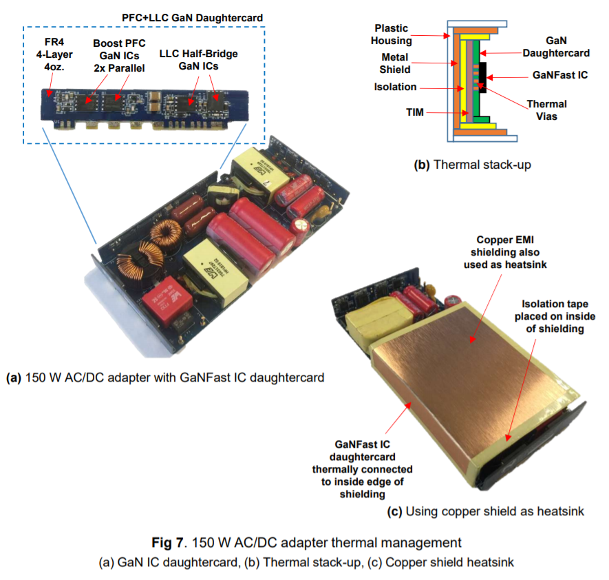
Thermal Management with Shielding
For larger power supply designs, a daughtercard with the GaNFast ICs can be inserted into the main power board along the edge. This allows for the heat from the GaNFast ICs to transfer through the thermal vias of the daughtercard to the backside copper planes. From the copper planes, a heatsink or airflow can then be attached for cooling. The following 150 W AC/DC adapter example (Figure 7) uses a thermal interface material (TIM) to conduct heat from the back of the
daughtercard to the copper shielding of the adapter. The internal adapter shielding is already necessary for EMI so it can also be used as a heatsink. The heat will then conduct from the shielding to the outside surface of the surrounding plastic housing
Revised 3-13-19

Page 7

Application Note AN010
Thermal Management with Shielding (cont.)
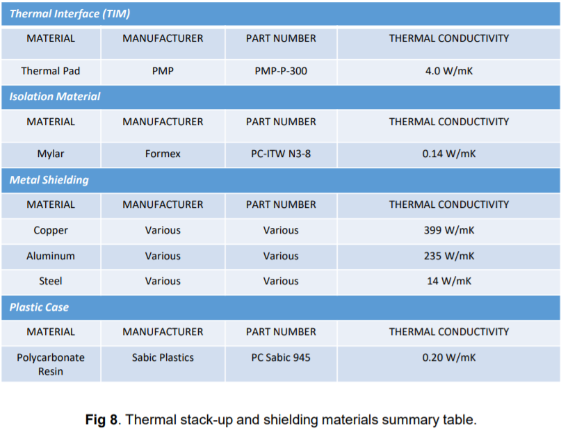
Materials commonly used for shielding include copper or aluminum. Steel can be also be used for improved EMI shielding and is typically tin-plated to prevent rusting or corrosion. Some available thermal stack-up and shielding materials are summarized in the table below (Figure 8).
Additional Information
DISCLAIMER Navitas Semiconductor Inc. (Navitas) reserves the right to modify the products and/or specifications described herein at any time and at Navitas’ sole discretion. All information in this document, including descriptions of product features and performance, is subject to change without notice. Performance specifications and the operating parameters of the described products are determined in the independent state and are not guaranteed to perform the same way when installed in customer products. The information contained herein is provided without representation or warranty of any kind, whether express or implied. This document is presented only as a guide and does not convey any license under intellectual property rights of Navitas or any third parties.
Navitas’ products are not intended for use in applications involving extreme environmental conditions or in life support systems.
Products supplied under Navitas Terms and Conditions.
Navitas Semiconductor, Navitas, GaNFast and associated logos are registered trademarks of Navitas.
Copyright ©2019 Navitas Semiconductor Inc. All rights reserved
Navitas Semiconductor Inc., 2101 E El Segundo Blvd, Suite 201, El Segundo, California 90245, USA.
Contact [email protected]
Revised 3-13-19

Page 8