APEC 2022 IS13 Sinow/Giandalia – Advancements in GaN Power IC System Integration
![27_Pdf_File_Type_Adobe_logo_logos-512[1]](https://navitassemi.com/wp-content/uploads/2020/12/27_Pdf_File_Type_Adobe_logo_logos-5121.png)


Advancements in
GaN Power IC System Integration
Victor Sinow, Sr. Principal Design Engineer Marco Giandalia, VP IC Design Navitas Semiconductor
[email protected] , [email protected]
The Integration Journey
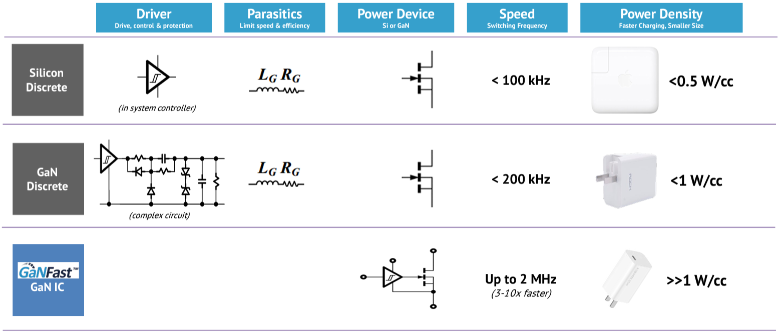
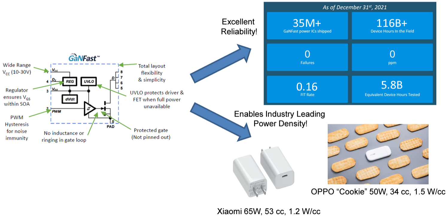
Navitas Generation 2 – GaNFast
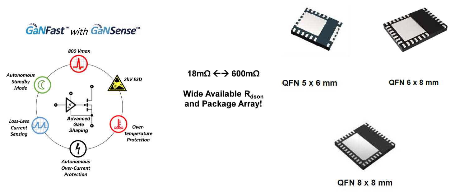
Navitas Generation 3 – GaNSense
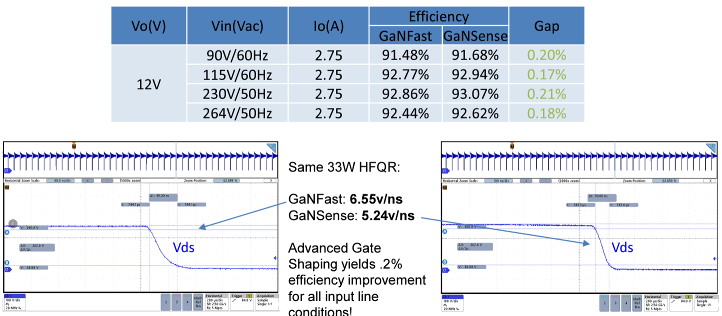
Advanced Gate Shaping
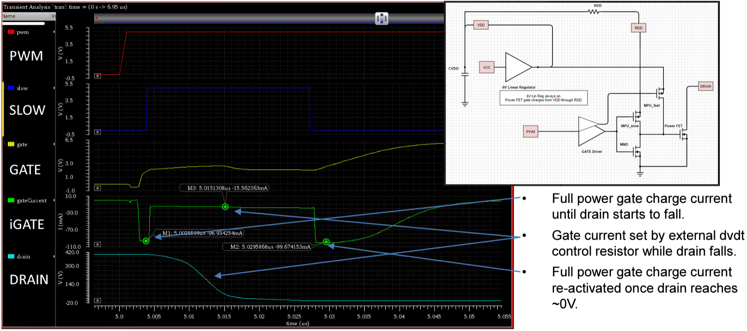
Advanced Gate Shaping – Effect
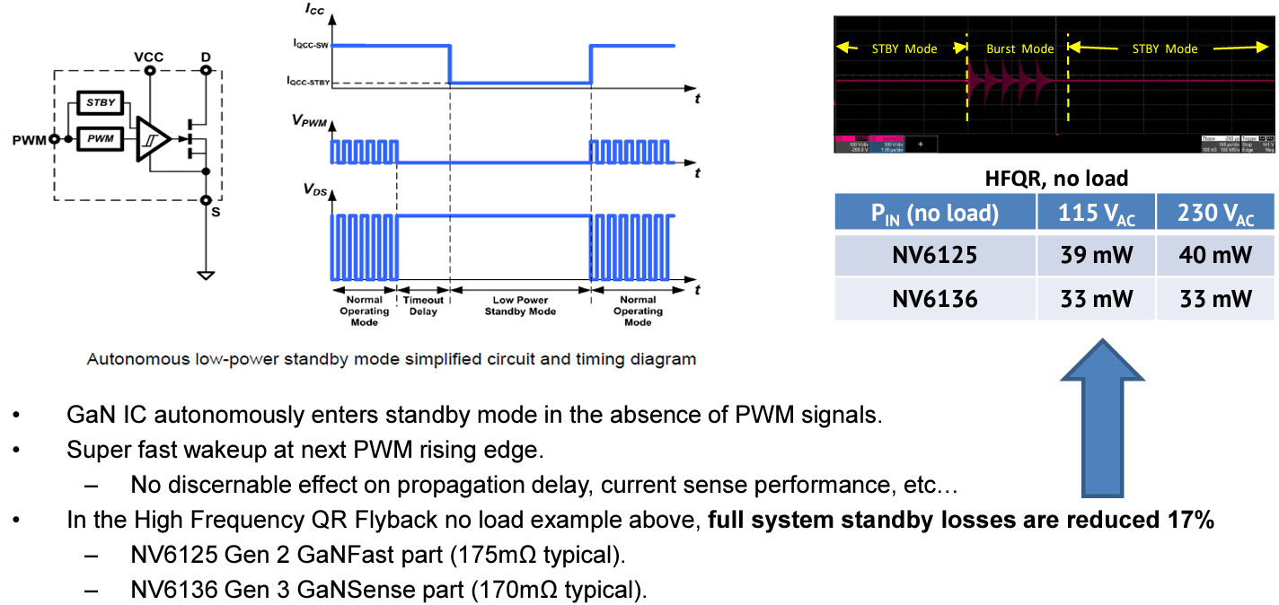
Autonomous Standby Mode
Lossless Current Sensing – What Is It?
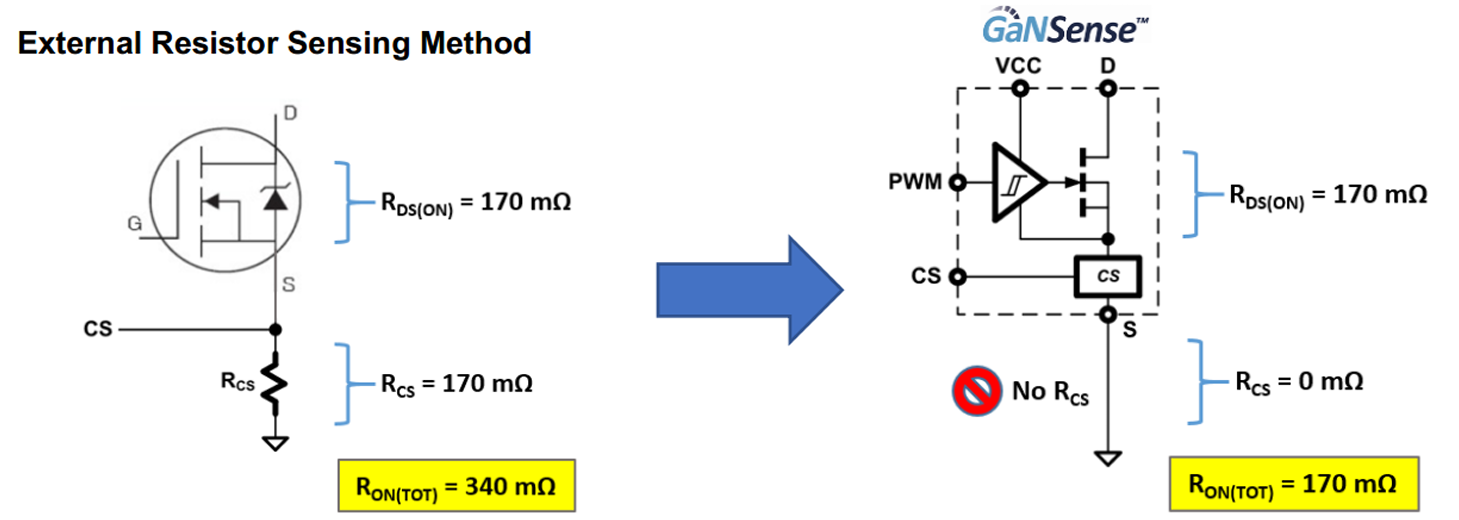
• Reduce RDS(ON)_TOTAL by 50%
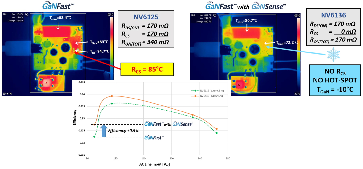
• Efficiency increased +0.5%
• No RCS PCB hotspot (-85°C)
• No RCS PCB footprint (-30 mm2)
Lossless Current Sensing – Does It Work?
Lossless Current Sensing – Details
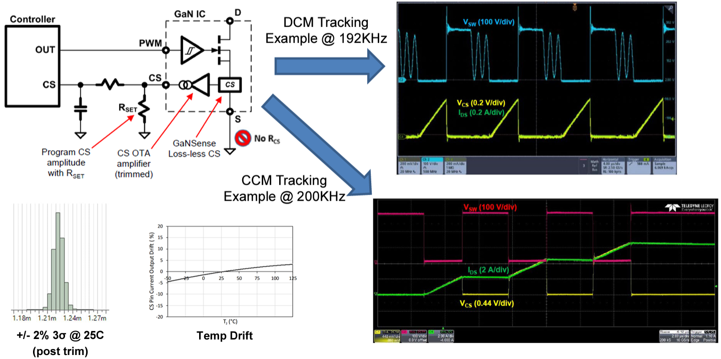
Autonomous Over Current Protection (OCP)

• On any given cycle, if the CS output voltage exceeds 1.9V, the internal gate driver will turn off the GaN IC and truncate the on-time.
– OCP response time 30ns! Compare to ~200ns response if relying on most conventional controllers.
• The current at which the IC protects is dependent on the IDRAIN→ ICS ratio and the value of RSET.
• Turn-on OCP blanking time prevents noise from triggering the fault and is optimized for GaN FET protection.
• This protection mechanism is designed to be accurate and user programmable via RSET.
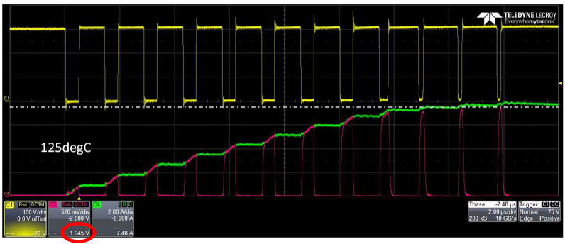
Autonomous OCP Over Temperature

GaNSense 260mΩ in double pulse tester:
• CS signal matches IDS current, independent of temperature.
• OCP uses CS signal, and the trip point is consistent over temperature.
• OCP is cycle by cycle, and limits inductor current.
• Conduction time when turning on into an OCP condition is equal to the optimized blanking interval.
Saturation Detection for Short Circuit Protection

• On any given cycle, if VDS of the GaN FET exceeds VISAT+, the internal gate driver will turn off the GaN IC and truncate the on-time.
• Turn-on ISAT blanking time prevents noise from triggering the fault and is optimized for GaN FET protection.
• This protection mechanism is designed for catastrophic events such as input to drain shorts, half bridge shoot through failure, saturated power inductance, etc…
Over Temperature Protection (OTP)
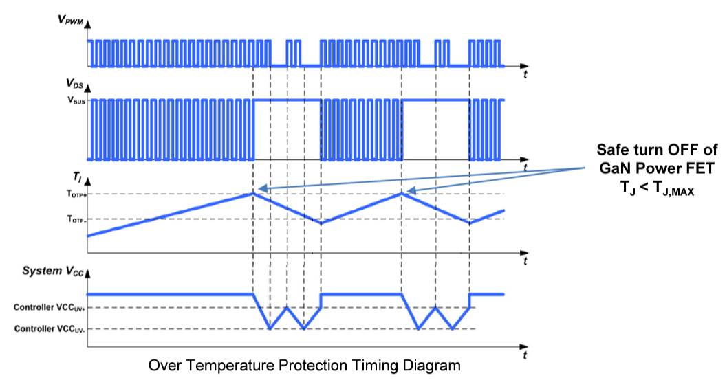
• Should TJ exceed the internal TOTP+ threshold (165 ℃, typical) then the IC will latch off safely.
• When TJ decreases again and falls below the internal TOTP- threshold (105 ℃, typical), the OTP latch will be reset.
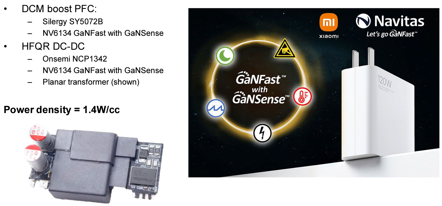
GaNSense In Mass Production (1)
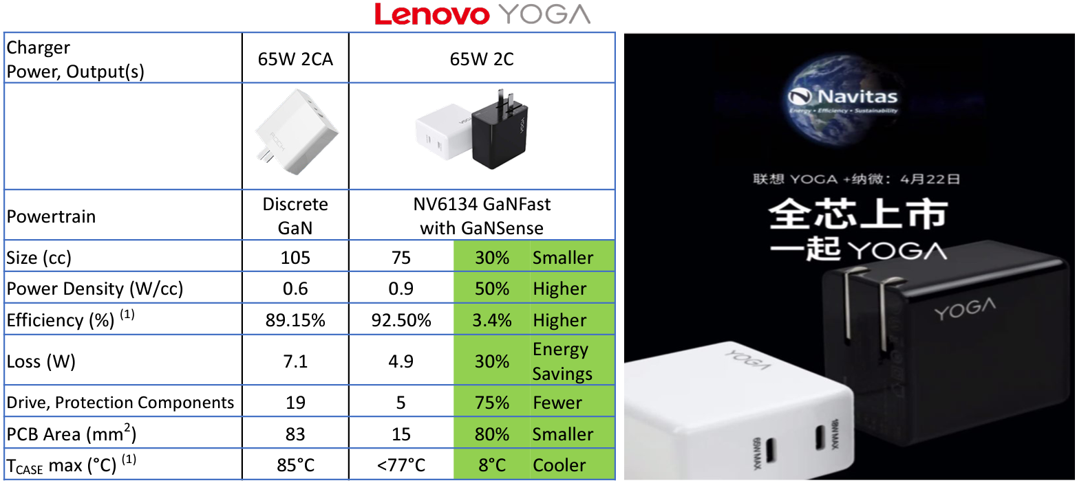
GaNSense In Mass Production (2)
Presenter Bios

• Victor Sinow is a Senior Principal Engineer at Navitas Semiconductor and serves as the Lead Power IC Architect for the company. Victor has been in the power semiconductor / systems space for more than 12 years and holds both a BS EE and an MS EE from MIT.
• Victor’s previous experience includes (1) designing and bringing to market the Dart 65W power adapter in his roles first as a Principal Engineer and then as the Director of the Power Engineering group at FINsix Inc; (2) designing various control ICs for offline power converters while working as an IC design engineer in the Power Supply Control group at Texas Instruments.
• Victor has been granted patents for innovations in circuit topologies, power system solutions, and semiconductor devices.

• Marco Giandalia serves as Vice President IC Design for Navitas Semiconductor and has 25 years experience in the field of Power IC products and technology development in Si and GaN since he received is MSEE in 1996.
• Before joining Navitas, Marco led the Energy Saving Product- Design Center at International Rectifier developing innovative products for Off-Line application like motor drive, AC/DC, DC/DC converters. Earlier he was in charge as IC Design Engineer at STMicroelectronics for Smart Power IC product line.
• He has been granted several patents for Power IC design solutions and has been author of multiple papers and conferences presentations