NV6169 PQFN 8×8 GaNFast™ Power IC with GaNSense™ Technology for Higher-Power Applications
By Tom Ribarich, Sr. Director Strategic Marketing

Navitas GaNFast Power ICs with GaNSense technology include control, drive, sensing and protection features for 30 W to 1 kW applications across mobile, consumer, industrial, data center and enterprise market segments. Integrated gate-drive eliminates parasitic gate-loop inductance and prevents gate ringing and glitching. Integrated, loss-less current-sensing eliminates external current sensing resistors to increase system efficiency, reduce PCB footprint, eliminate R
CS hot-spots, and provides real-time overcurrent (OCP) and over-temperature protection (OTP) to deliver fast and reliable protection against shortcircuit and overload fault conditions. The NV6169 further expands the GaNSense product family into higher power applications with a low 45 mΩ R
DS(ON) and a new PQFN 8×8 mm package with a large cooling pad for excellent thermal management.
This application note includes a detailed description of the NV6169 and GaNSense functions, schematics and PCB layout guidelines, in-circuit examples and waveforms, and thermal management instructions. These guidelines are intended to achieve maximum efficiency and power density and to enable the highest level of system robustness and reliability.
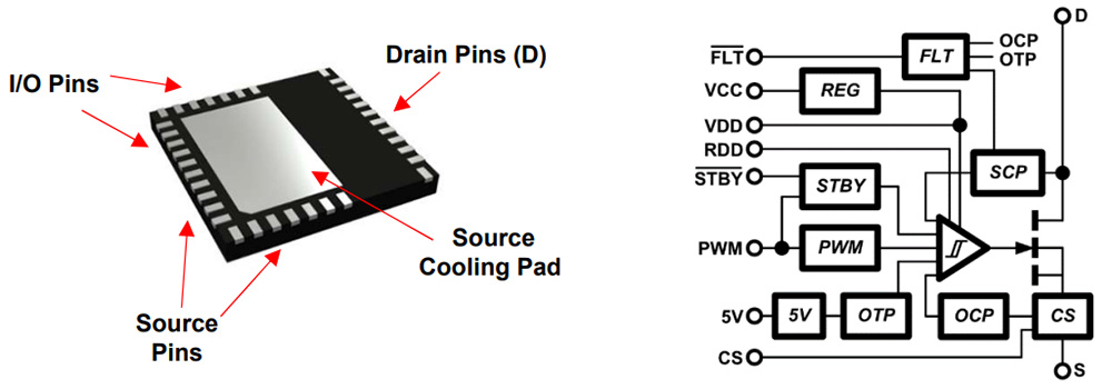
GaNFast Power ICs have been designed into a variety of high-density power supplies due to integrated gate drive, wide range VCC and PWM inputs, internal ESD protection, and large thermal cooling pad. GaNSense technology has provided another layer of key features such as loss-less current sensing, OCP, OTP, and auto-standby mode, that have increased system robustness and reliability, increased system efficiency and reduced standby power. These GaN Power ICs have enabled high-frequency operation with ease-of-use, design flexibility and compatibility with all popular topologies and controllers. To further expand the GaNSense product family into higher power applications, the NV6169 45 mΩ version has been developed in a PQFN 8×8 package. The IC pinout of the NV6169 includes (see Fig. 1) Drain pins (D), Source pins (S), I/O pins, and a large Source cooling pad. The I/O pins include IC supply pins, PWM input, dV/dt turn-on control, current-sensing output and fault output. Most of the switching currents of the external power conversion circuit flow from the Drain pins, through the GaN power FET, and to the Source pins. Heat generated from the GaN IC must be taken out through the Source cooling pad and to the PCB. Large PCB copper areas and thermal vias are then used to transfer the heat to the opposite side of the PCB and/or to inner layers that have large copper planes where it can then be spread and cooled. The cooling pad is conveniently connected to PGND to gain additional PCB thermal copper area.

Figure 1: NV6169 PQFN 8×8 package bottom view (left) and simplified schematic (right)
IC Pins, Connections and Components
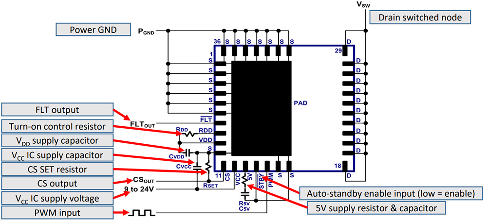
The typical connection diagram for this GaN IC is shown in Fig. 2. The IC pins include drain of the GaN IC (D), source of the GaN IC (S), IC supply (VCC), gate drive supply (VDD), gate drive turn-on control SET input (RDD), PWM input (PWM), fault output (FLT), current sensing output (CS), auto-standby mode input (STBY) and 5V supply (5V). The Source PAD and Source (S) pins 1-6, 30-36, should all be connected to the system PGND. Source (S) pins 10,16,17, can be used for local GND connections for the IC external components. The Source pins (S) are connected to the Source pad internally, but it is good practice to also connect the Source pins to the Source pad externally (see PCB Layout Guidelines, Page 11). The Drain Pins (D) 18-29 are connected internally and it is also good practice to connect externally. The external components around the IC include VCC filter capacitor (CVCC) connected from VCC pin to Source (S), VDD filter capacitor (CVDD) connected from VDD pin to Source (S), turn-on dV/dt set resistor (RDD) connected from VDD pin to RDD pin, current-sense amplitude-set resistor (RSET) connected from CS pin to Source (S), and auto-standby mode enable pin (STBY) connected to Source (S). A series resistor (R5V, 10 Ω typ.) and capacitor (C5V, 0.01uF typ.) are required from pin 5V to Source (S). The 5V pin is for internal purposes only and must not be used for biasing external circuitry. The table below (Table I) shows the recommended component values (typical only) for the external components connected to the pins of this GaN IC. These components should be placed as close as possible to the IC.

Figure 2: GaN IC connection diagram
Table 1: Recommended component values (typical only)
Loss-Less Current-Sensing
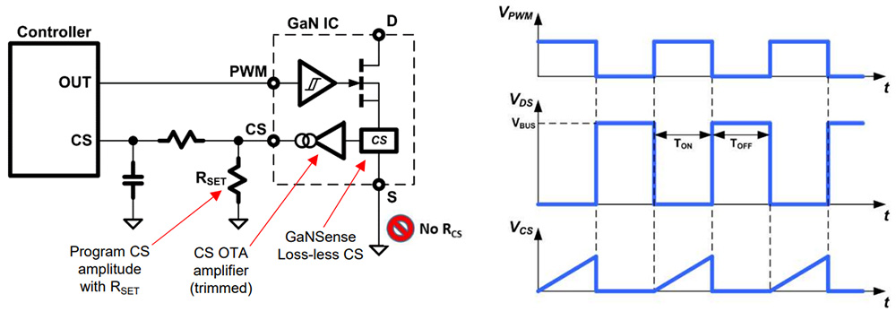
For many applications it is necessary to sense the cycle-by-cycle current flowing through the GaN IC. Existing current-sensing solutions include placing a series-current-sensing resistor in between the Source connection of the power FET and PGND. Using external current-sensing resistors increases system conduction power losses, creates a hot-spot on the PCB, and lowers overall system efficiency. To eliminate external resistors and hot-spot, and increase system efficiency, this GaN IC integrates accurate and programmable loss-less current-sensing. The IDS current flowing through the GaN IC is sensed internally (Fig. 4) and then amplified, trimmed and converted to a current at the current-sensing output pin (CS). An external resistor (RSET) is connected from the CS pin to the SGND pin and is used to set the amplitude of the CS pin voltage signal. This allows for the CS pin signal to be programmed to work with different controllers with different current-sensing input thresholds.

Figure 4: Loss-less current sensing circuit and timing diagram
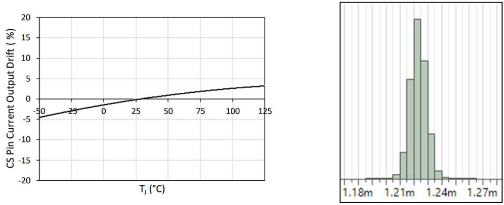
Due to careful design of internal current-sensing and amplifier circuits, plus accurate test and trim in production, the accuracy of the internal current-sensing circuit is very high (Fig. 5). The CS pin current versus temperature graph illustrates the normal positive temperature coefficient behavior of the internal circuit, with a +/- 4% tolerance from -40 to 125°C.
Figure 5: CS pin current vs TCASE and post-trim production data (typical only)
Loss-Less Current Sensing (cont.)
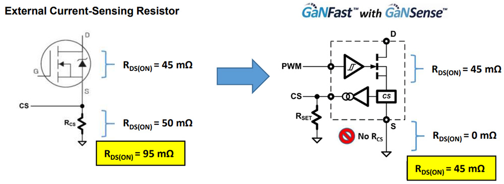
When comparing GaNSense technology versus an existing external resistor-sensing method (Fig. 6), the total ON resistance, RON(TOT), can be substantially reduced. For a 300 W high-frequency boost PFC circuit, for example, RON(TOT) is reduced from 95 mΩ to 45 mΩ. The power loss saving by eliminating the external resistor results in a +0.2% efficiency benefit for the overall system and eliminates the PCB hotspot (> 85 °C) from external RCS resistors.
Figure 6: External resistor-sensing vs. GaNSense technology
To select the correct RSET resistor value, the following equation (Equation 1) can be used. This equation uses the equivalent desired external current-sensing resistor value (RCS), together with the gain of the internal sensing circuitry. This RSET value will then give the correct voltage level at the CS pin to be compatible with the internal current sensing threshold of the system controller.
Equation 1: RSET resistor value equation
Loss-Less Current-Sensing (cont.)
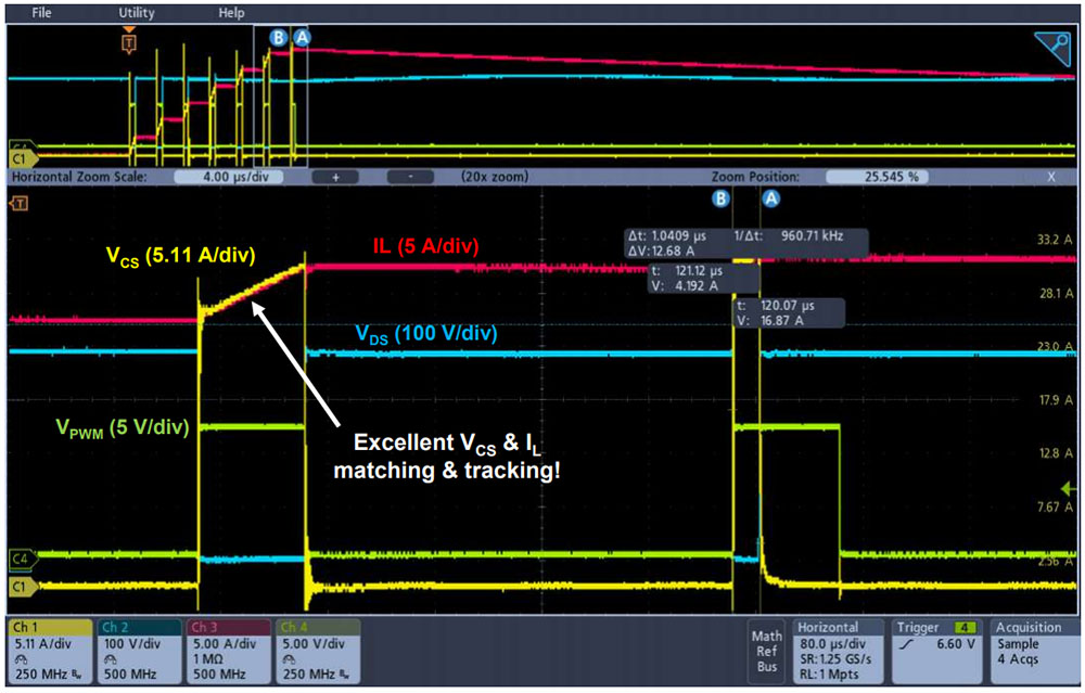
During bench testing, the switching waveforms (Fig. 7) show the CS pin tracking performance versus inductor current (IL) during inductive switching boost CCM conditions. The switching performance shows excellent VCS and IL real-time matching and tracking at 30 A current levels. To show tracking accuracy, the CS pin voltage scale for all waveforms is based on RCS gain calculation to match current probe scale.
Figure 7: Loss-less current-sensing waveforms (Inductive switching boost CCM)
Over Current Protection (OCP)
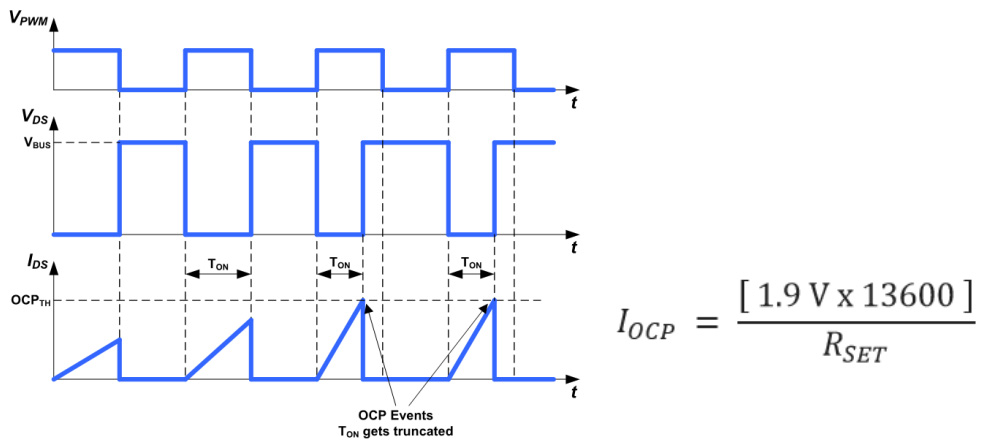
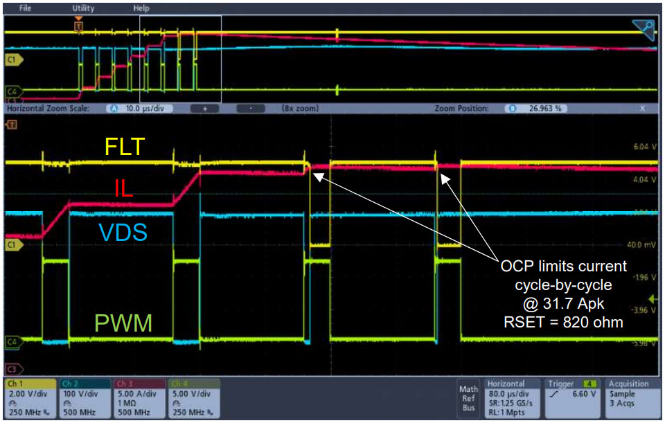
This GaN IC includes cycle-by-cycle over-current detection and protection (OCP) circuitry to protect the GaN IC against high current levels. During the on-time of each switching cycle, should the peak current exceed the internal OCP threshold (1.9 V, typical), then the internal gate drive will turn the GaN IC off quickly and truncate the on-time period to prevent damage from occurring to the IC. The IC will then turn on again at the next PWM rising edge at the start of the next on-time period (Fig. 8). This OCP protection feature will self-protect the IC each switching cycle against fast peak over current events and greatly increase the robustness and reliability of the system. The OCP threshold equation (Fig. 8) is a function of the internal current-sensing ratio and the external RSET resistor and can be used to program the desired OCP current limit level. The internal OCP threshold (1.9 V, typical) is much higher than the OCP thresholds of many popular boost PFC controllers. This ensures good compatibility of this IC with existing controllers without OCP threshold conflicts. Fig. 9 shows measured waveforms during cycle-by-cycle OCP limitation during inductive switching (boost CCM). The FLT output can also be seen going low each cycle during each OCP event.

Figure 8: OCP timing diagram & OCP threshold equation
Figure 9: Over-current cycle-by-cycle limitation during boost CCM
Over-Temperature Protection (OTP)
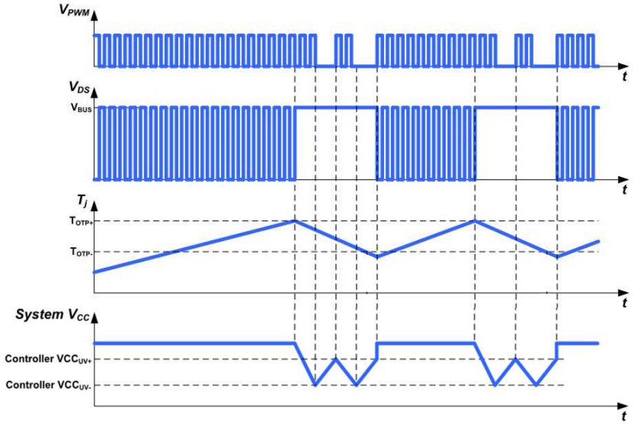
The NV6169 includes over-temperature detection and protection (OTP) circuitry to protect the IC against excessively high junction temperatures (TJ). High junction temperatures can occur due to overload, high ambient temperatures, and/or poor thermal management. Should TJ exceed the internal TOTP+ threshold (165℃, typical) then the IC will latch off safely (Fig. 10). When TJ decreases again and falls below the internal TOTP- threshold (105℃, typical), then the OTP latch will be reset. Until then, internal OTP latch is guaranteed to remain in the correct state while VCC is greater than 5 V. During an OTP event, this GaN IC will latch off and the system VCC supply voltage can decrease due to the loss of the aux winding supply. The system VCC will fall below the lower UV- threshold of the system controller and the system high voltage start-up circuit will turn-on and VCC will increase again (Fig. 10). VCC will increase above the rising UV+ threshold and the controller will turn on and deliver PWM pulses again but the NV6169 will remain off until TJ has decreased below TOTP- and the OTP fault latch is reset. Once the fault latch is reset, this GaN IC will start switching again at the next PWM pulses from the controller. During an OTP fault condition, the FLT output will go low and will remain low during the complete OTP fault condition.

Figure 10: OTP timing diagram
Programmable Turn-on dV/dt Control
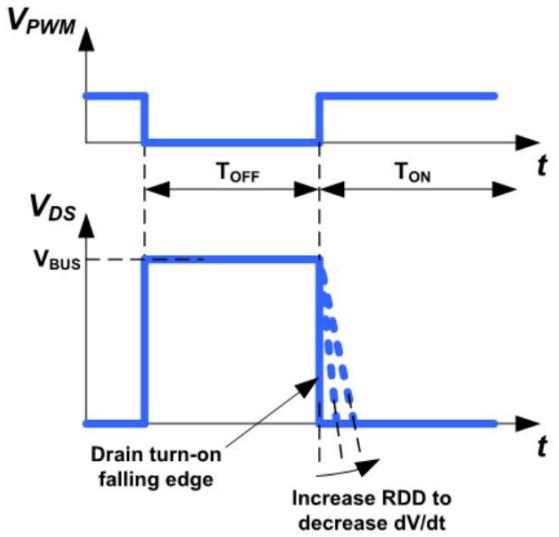
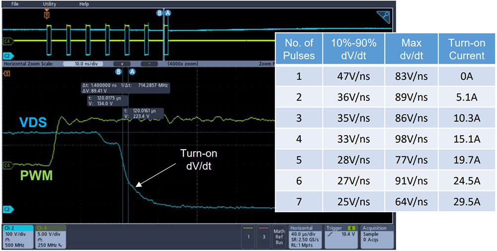
During first start-up pulses or during hard-switching conditions, it is desirable to limit the slew rate (dV/dt) of the drain of the GaN IC during turn-on. This is necessary to reduce EMI or reduce circuit switching noise. To program the turn-on dV/dt rate of the GaN IC, a resistor (RDD) is placed between the VDD pin 30 and the RDD pin 29 (see Fig. 2). This resistor (RDD) sets the turn-on current of the internal gate driver and therefore sets the turn-on falling edge dV/dt rate of the drain of the power FET (Fig. 11). The actual VDS waveform and dV/dt rates vs different turn-on current values are also shown (Fig. 12).
Figure 11: Turn-on dV/dt slew rate control simplified timing diagram
Figure 12: VDS turn-on slew rates (dV/dt) waveforms at different turn-on current levels (Inductive switching boost CCM)
Autonomous Low-Power Standby Mode
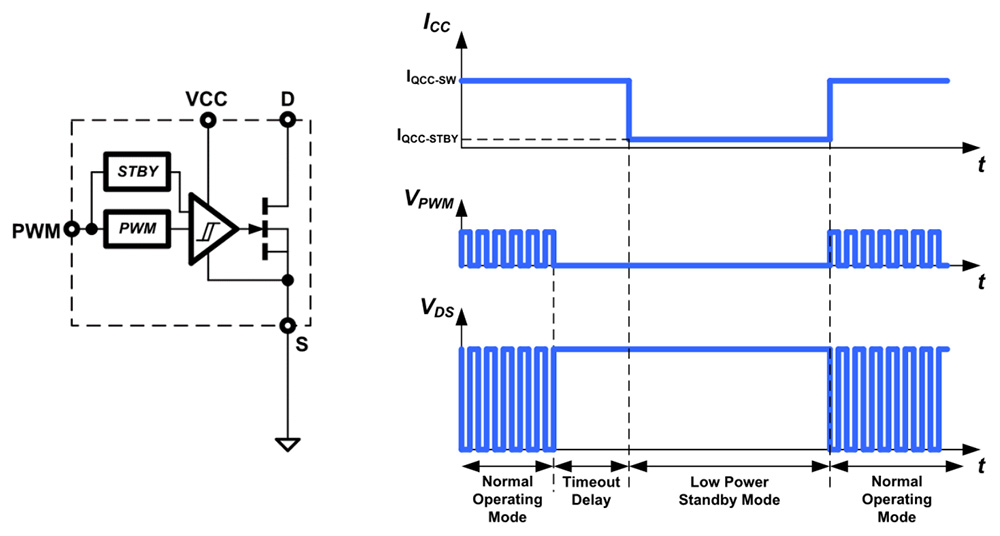
This GaN IC includes an autonomous low-power standby mode for disabling the IC and reducing the VCC current consumption. During normal operating mode, the PWM pin toggles high and low to turn the GaN IC on and off. If the input pulses at the PWM pin stop and stay below the lower VPWML turn-off threshold (1.1 V, typical) for the duration of the internal timeout standby delay (tTO_STBY, 90 us, typical), then the IC will automatically enter low power standby mode (Fig. 13). This will disable the gate drive and other internal circuitry and reduce the VCC supply current to a low level (255 uA, typical). When the PWM pulses restart, the IC will wake up at the first rising edge of the PWM input and enter normal operating mode again. To enable autonomous standby mode, the auto-standby mode pin 14 (STBY) should be set ‘low’ and connected to the nearest Source (pin 16). To disable autonomous standby mode, STBY pin 14 should be set ‘high’ and connected to the adjacent 5 V pin 13.

Figure 13: Autonomous low-power standby mode simplified circuit and timing diagram
PCB Layout Guidelines (PQFN 8×8 mm)
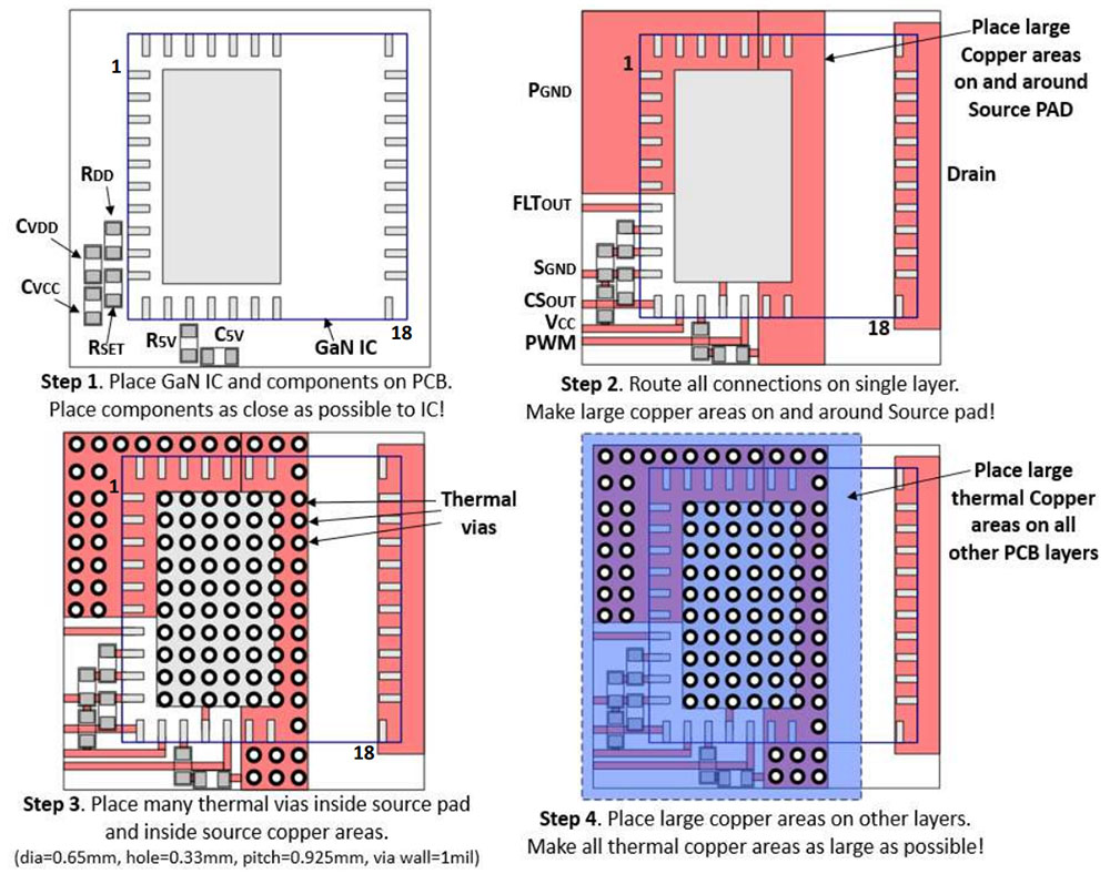
For best electrical and thermal results, these PCB layout guidelines and the 4 steps highlighted below must be followed:
1) Place IC components as close as possible to the GaN IC. Place RSET resistor directly next to CS pin to minimize high frequency switching noise.
2) Connect the ground of IC components to Source pin 10 or Source pin 17 to minimize high frequency switching noise.
3) Route all connections on single layer. This allows for large thermal copper areas on other layers.
4) Place large copper areas on and around Source pad.
5) Place many thermal vias inside Source pad and inside source copper areas.
6) Place large as possible copper areas on all other layers (bottom, top, mid1, mid2).
Figure 14: PCB layout steps
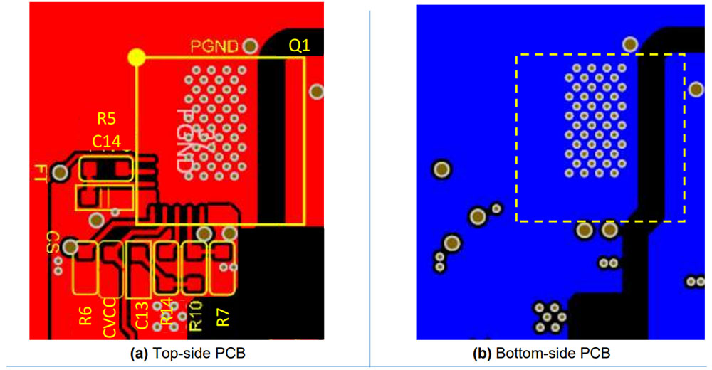
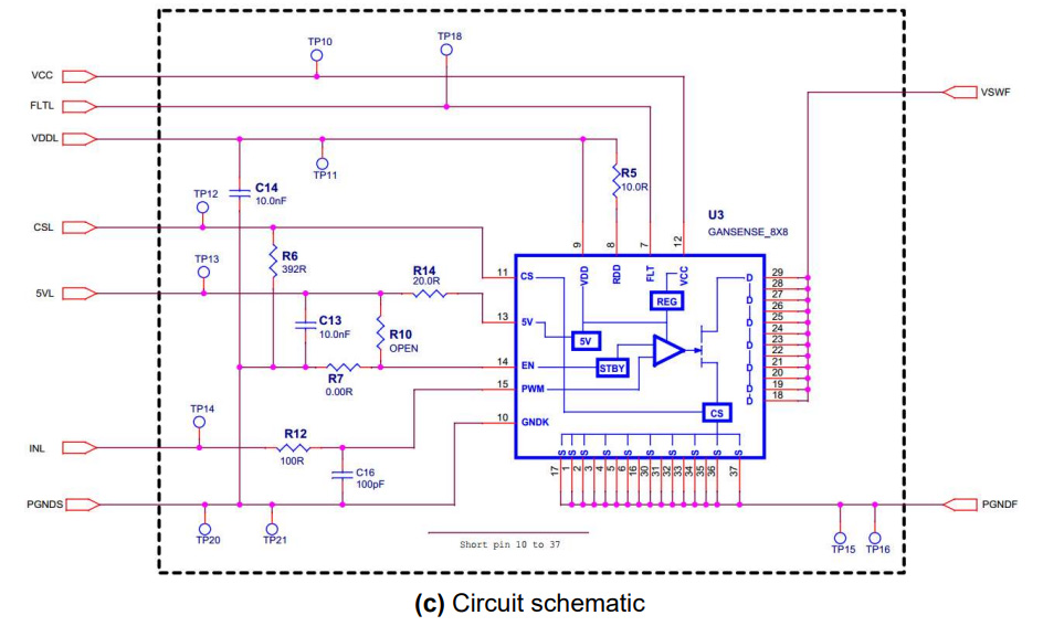
The following example (Fig. 15) shows PCB test board example of proper layout practices for NV6169 PQFN 8×8 mm. All components are placed and routed on the top layer allowing all other layers to be used for large copper area and thermal vias. If a 4-layer PCB is used, then additional thermal copper area can be gained.
Figure 15: PCB and layout example for GaN IC. (a) Top-side PCB, (b) Bottom-side PCB, (c) Circuit schematic
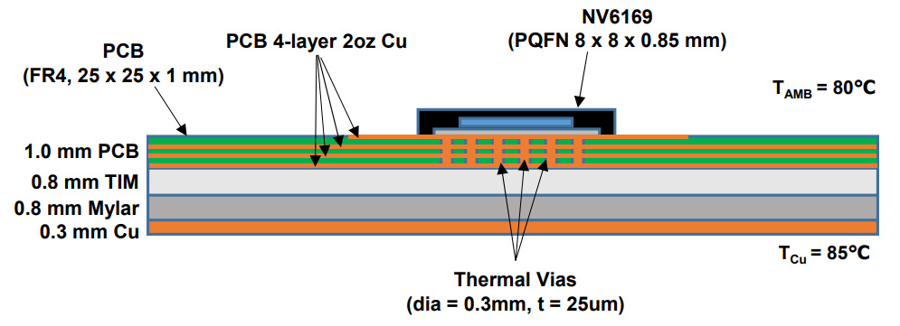
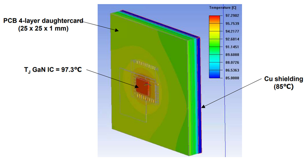
The following thermal model (Fig. 16) is for a PCB daughtercard with the GaN IC mounted on one side of the PCB. The heat from the GaN IC flows through the package leadframe, to the PCB copper layers and vias, through the thermal interface material (TIM) and laterally through the PCB to the sides. The TIM then goes to the safety insulating material (Mylar) and then to a Cu shield (used for heatsinking and EMI suppression). The thermal conductivity for these materials are listed in Figure 18. To represent the actual thermal conditions inside a 300W charger running at full load, the Cu shield is held at 85℃, the TAMB is set at 80℃, and PLOSS for the GaN IC is set at 1 W. From the thermal simulation (Fig. 17), the TJ of the GaN IC reaches approx. 97.3℃. This result looks reasonable for the GaN IC running during worst case line, load and ambient temperature conditions. Further improvement of the GaN IC temperature is possible by using TIM with higher conductivity and by using thinner Mylar (if safety conditions allow).

Figure 16: Daughtercard thermal model stack-up diagram
Figure 17: Daughtercard 3D thermal simulation (PLOSS_GaN = 1 W, TAMB = 80℃)
Thermal Management (cont.)
Materials commonly used for shielding include copper or aluminum. Steel can be also be used for improved EMI shielding and is typically tin-plated to prevent rusting or corrosion. Some available thermal stack-up and shielding materials are summarized in the table below (Figure 18).
Figure 18: Thermal stack-up and shielding materials summary.
References (www.navitassemi.com)
1) GaNFast NV6123, NV6125, NV6127 datasheets, Navitas Semiconductor, 2019
2) Thermal Management of GaNFast Power ICs, AN010, Navitas Semiconductor, 2019
3) GaNFast NV613x/NV615x, NV6169 Power ICs with GaNSense Technology datasheets, Navitas Semiconductor, 2021/2022
4) New GaNFast Power ICs with GaNSense Technology Loss-Less Current Sensing & Autonomous Protection, AN015, Navitas Semiconductor, 2021
DISCLAIMER Navitas Semiconductor (Navitas) reserves the right to modify the products and/or specifications described herein at any time and at Navitas’ sole discretion. All information in this document, including descriptions of product features and performance, is subject to change without notice. Performance specifications and the operating parameters of the described products are determined in the independent state and are not guaranteed to perform the same way when installed in customer products. The information contained herein is provided without representation or warranty of any kind, whether express or implied. This document is presented only as a guide and does not convey any license under intellectual property rights of Navitas or any third parties. Navitas’ products are not intended for use in applications involving extreme environmental conditions or in life support systems. Terms and Conditions.
Navitas Semiconductor, Navitas, GaNFast, GaNSense and associated logos are registered trademarks of Navitas. Copyright ©2023 Navitas Semiconductor. All rights reserved Contact: [email protected]
![27_Pdf_File_Type_Adobe_logo_logos-512[1]](https://navitassemi.com/wp-content/uploads/2020/12/27_Pdf_File_Type_Adobe_logo_logos-5121.png)

