New GaNFast™ Half-Bridge Power ICs with GaNSense™ Technology
By Tom Ribarich, Sr. Director Strategic Marketing
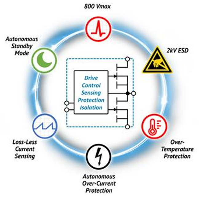
NV624x GaNFast half-bridge ICs with GaNSense includes two GaNFETs and drivers, pluscontrol, level-shifting, sensing and protection features for 65-300 W applications across mobile, consumer and industrial markets. Comprehensive integration delivers high reliability, efficiency and density, and creates an easy-to-use system building block.
- Reliability: No gate ringing and glitching due to monolithic integration of GaNFET and GaNdriver (no parasitic gate-loop inductance). Real-time over-current (OCP) and over-temperature protection (OTP) deliver fast and reliable protection against short-circuit and overload fault conditions plus wide-range VCC, 2kV ESD protection, shoot-through protection, and UVLO are included.
- Efficiency: Loss-less current-sensing eliminates external current-sensing resistors (RCS) to increase system efficiency, reduce PCB footprint and eliminate RCS hot-spots. A thermally-enhanced 6x8mm PQFN package with dual large cooling-pads enables a small PCB footprint with excellent cooling, and auto-standby mode reduces off- or sleep-state losses.
- Easy-to-use: Simple, independent, low-side-referenced PWM inputs feed an integrated level-shifter and bootstrap for isolated, high-and low-side half-bridge switching. 45% fewer external components and PCB area than discrete designs, and standard QFN package enable shorter design-times and maximized chance of first-time-right.
GaNFast half-bridge ICs enable high-frequency, soft-switching topologies such as active-clamp flyback (ACF), asymmetrical half-bridge (AHB), resonant LLC, totem-pole PFC (TTP) which are critical for highest efficiency, power density and system cost. Robust hard-switching performance and rich features increase switching frequency and efficiency in 3-phase motor-drive applications. Each topology has unique benefits and are selected per system requirements and desired power level, which should be well defined, and the topology carefully selected before any design work is started.
This application note includes a detailed description of the IC features and functions, schematics and PCB layout guidelines, in-circuit examples and waveforms, and thermal management instructions. Electrical model simulation results are also included to help designers get their designs going quickly.
Figure 1: GaNFast half-bridge IC companion topologies and power levels
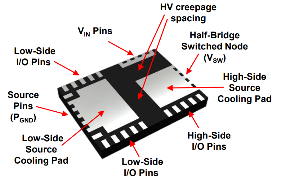
The IC integrates a complete half-bridge power-train together with level-shifting, bootstrap, two low-side GND-referenced PWM inputs, and low-side loss-less current-sensing. The IC pinout (see Fig. 2) includes high-voltage DC-bus input and high-side GaN power FET drain connection (VIN), high-side GaN power FET source pad and low-side GaN power FET drain connection (VSW), high-side I/O pins, low-side GaN power FET source pad (PGND) and low-side I/O pins. High-side I/O pins include the high-side IC supply pins, and low-side I/O pins include PWM inputs, dV/dt turn-on control, and current-sensing output. The complementary switching currents of the external power-conversion circuit flow through the drain-to source of both GaN power FETs. Heat generated from GaN power FETs is removed through both source cooling pads at the bottom side of QFN package to the PCB. Large PCB copper areas and thermal vias are then used to transfer the heat to the opposite side of the PCB and/or to inner layers that have large copper planes where it can then be spread and cooled. The low-side cooling pad is conveniently connected to PGND to gain additional PCB thermal copper area. The low-side source pad and I/O pins are separated from the high-side source pad and I/O pins by a sufficient high-voltage creepage distance.

Figure 2: GaNFast half-bridge IC PQFN 6×8 package highlights (bottom view)
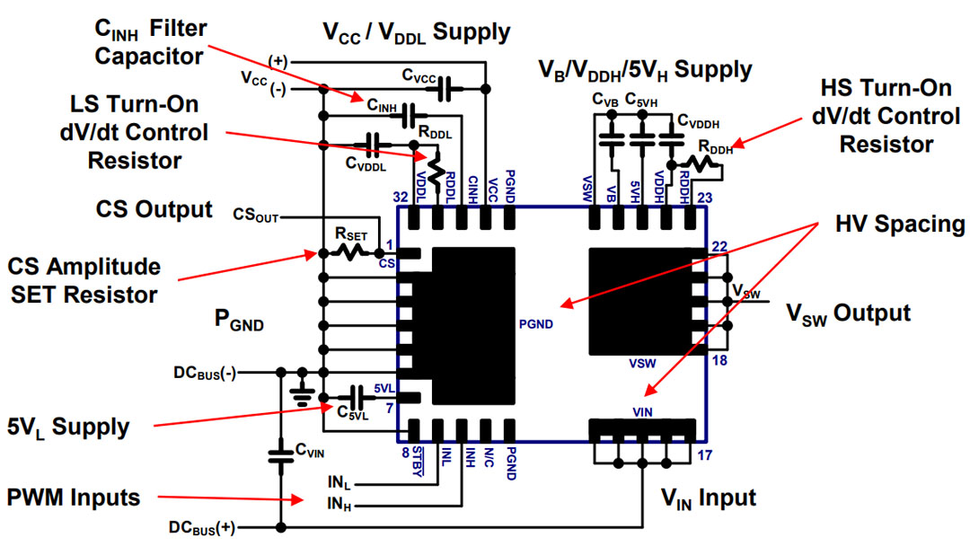
The typical connection diagram for this GaN Half-Bridge IC is shown in Figure 3. The IC pins include the drain of the high-side GaN power FET (VIN), the half-bridge mid-point switched node (VSW), the source of the low-side GaN power FET and IC GND (PGND), low-side IC supply (VCC), low-side gate drive supply (VDDL), low-side turn-on dV/dt control (RDDL), low-side 5V supply (5VL), low-side referenced PWM inputs (INL, INH), low-side current sensing output (CS), auto-standby enable input
(STBYN), high-side supply (VB), high-side gate drive supply (VDDH), and high-side 5V supply (5VH). The external low-side components around the IC include VCC supply capacitor (CVCC) connected between VCC pin and PGND, VDDL supply capacitor (CVDDL) connected between VDDL pin and PGND, turn on dV/dt set resistor (RDDL) connected between VDDL pin and RDDL pin, current sense amplitude set resistor (RSET) connected between CS pin and PGND, 5V supply capacitor (C5VL) connected between 5VL pin and PGND, the auto-standby enable pin (STBYN) connected to PGND to enable auto-standby mode or connected to 5VL to disable auto-standby mode, and the CINH filter capacitor connected between CINH pin and PGND, which is recommended for additional ground loop noise immunity (CINH). The external high-side components around the IC include VB supply capacitor (CVB) connected between VB pin and VSW, VDDH supply capacitor (CVDDH) connected between VDDH pin and VSW, turn-on dV/dt set resistor (RDDH) connected between VDDH pin and RDDH pin, and 5V supply capacitor (C5VH) connected between 5VH pin and VSW. The high side VB, 5VH and VDDH bypass capacitors must be chosen carefully to accommodate various system considerations such as high side wake up time, high side hold up time and standby power.

Figure 3: IC connection diagram
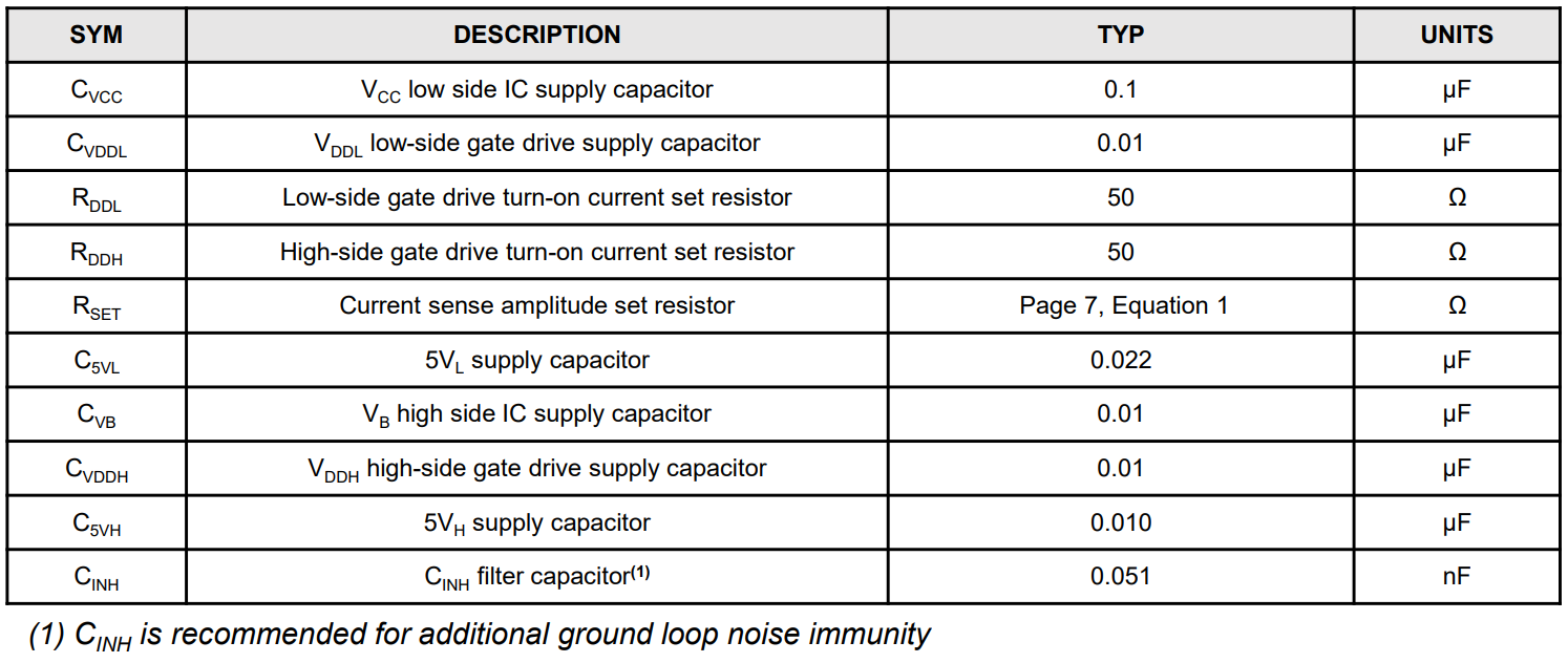
The following table (Table 1) shows the recommended component values (typical only) for the external components connected to the pins of the IC. These components should be placed as close as possible to the IC. Please see PCB Layout Guidelines for more information.
Table 1: Recommended component values (typical only)
Half-Bridge Daughter Card & Switching Waveforms
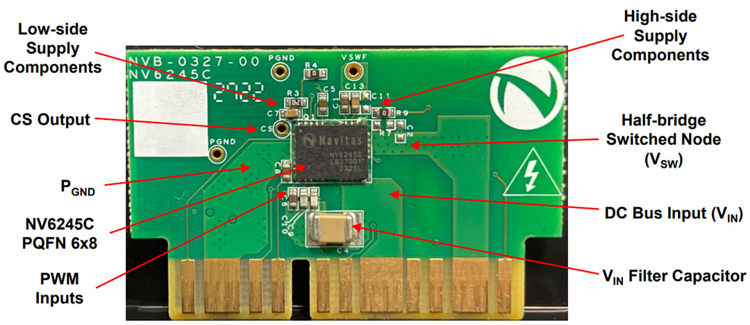
A multi-layer, half-bridge daughter card has been designed for bench testing purposes and to review the basic functionality and switching performance of the IC (Fig. 4). The daughtercard can be easily plugged into different application circuit motherboards, and includes the IC and all necessary external components. The external IC components have been placed and routed as close the IC as possible. Large copper planes and thermal vias have been placed on all layers at both source pads for good
thermal management. See PCB layout guidelines (page 13) for more information on proper PCB layout design.
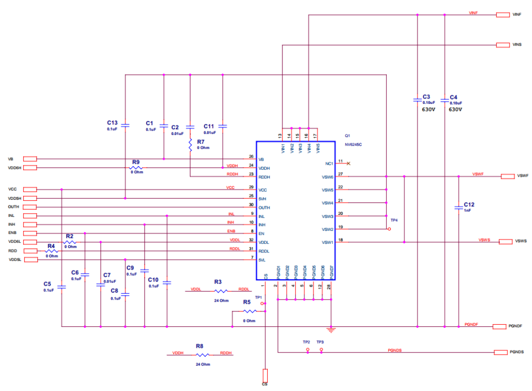
Figure 4: NV6245C GaNFast half-bridge IC daughtercard schematics and assembled PCB
Half-Bridge Switching Waveforms (cont.)
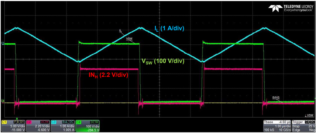
The basic switching waveforms (Fig. 5) during resonant ZVS conditions (FSW = 250 kHz, duty-cycle = 50%) include INL PWM input pulses, VSW half-bridge switched node output, and output inductor current (IL). The switching performance shows excellent on/off control of the integrated high- and low-side GaN power FETs. During the high-side on-time period (INH = high, INL = low), the high-side GaN power FET is turned on and the half-bridge switched node (VSW) is held at the VIN voltage level (DC bus voltage, 400 V). The output-inductor current ramps up to a positive peak level determined by one-half of the DC bus voltage level (+200 V), the inductor value, and the high-side GaN power FET on-time duration. When the high-side on-time period ends (INH = low, INL = low) the high-side GaN power FET turns off. During a short dead-time period, the inductor current slews the half-bridge switched-node down to PGND at a dV/dt rate determined by the positive peak inductor current value and the output capacitance of the GaN power FETs. At the end of the dead-time period, INL then turns on (INH = low, INL = high) and the low-side GaN Power FET turns on and holds the half-bridge switched node (VSW) at PGND. The inductor current ramps down to a negative peak level determined by negative one-half of the DC bus voltage level (-200 V), the inductor value, and the low-side GaN power FET on-time duration. When the low-side on-time period ends (INH = low, INL = low) the low-side GaN power FET turns off. During another short dead-time period, the inductor current slews the half-bridge switched node up to the VIN voltage level (400 V) at a dV/dt rate determined by the negative valley of the inductor current and the output capacitance of the GaN power FETs. The switching cycle then repeats and ZVS switching conditions are maintained each rising and falling edge of the half-bridge switched node (VSW).

Figure 5: GaNFast half-bridge IC basic switching waveforms (resonant ZVS mode, duty-cycle = 50%, FSW = 250 kHz)
Loss-Less Current-Sensing
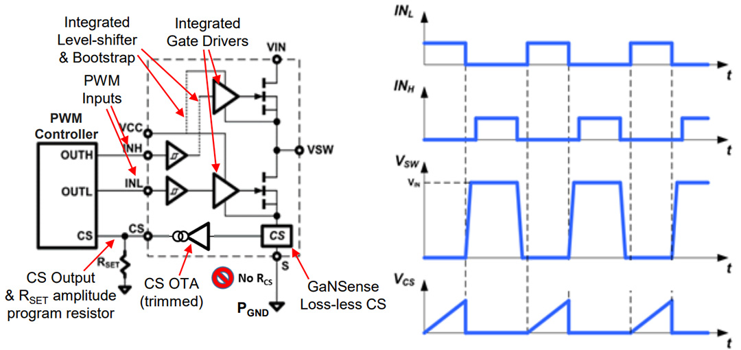
For many applications it is necessary to sense the cycle-by-cycle current flowing through the low-side GaN power FET. Existing current-sensing solutions include placing an external current-sensing resistor in between the source connection of the low-side power FET and PGND. Using external current-sensing resistors increases system conduction power losses, creates a hot-spot on the PCB, and lowers overall system efficiency. To eliminate external resistors and hot-spot, and increase system efficiency, the IC integrates accurate and programmable loss-less current-sensing. The IDS current flowing through the lowside GaN power FET is sensed internally (Fig. 6) and then amplified, trimmed and converted to a current at the current-sensing output pin (CS). An external resistor (RSET) is connected from the CS pin to the PGND pin and is used to set the amplitude of the CS pin voltage signal. This allows for the CS pin signal to be programmed to work with different controllers with different current-sensing input thresholds.

Figure 6: IC simplified internal block diagram & timing diagram
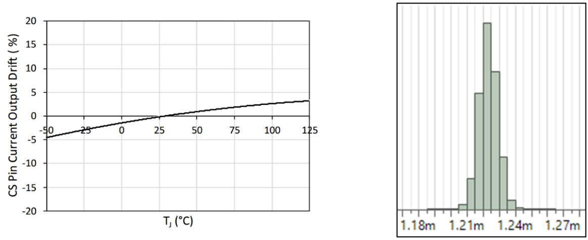
Due to careful design of internal current-sensing and amplifier circuits, plus accurate test and trim in production, the accuracy of the internal current-sensing circuit is very high (Fig. 7). The CS pin current versus temperature graph illustrates the normal positive temperature coefficient behavior of the internal circuit, with a +/- 4% tolerance from -40 to 125°C.
Figure 7: CS pin current vs TCASE and post-trim production data (typical only)
Loss-Less Current Sensing (cont.)
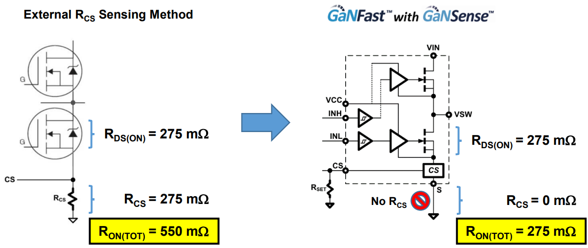
When comparing GaNSense technology versus existing external current sensing resistor method (Fig. 8), the total ON-resistance, RON(TOT), can be substantially reduced. For a 65 W, high-frequency ACF circuit, for example, RON(TOT) is reduced from 550 mW to 275 mW. The power loss savings by eliminating the external resistor results in a +0.5% efficiency benefit for the overall system
Figure 8: External resistor-sensing vs. GaNSense loss-less current sensing
To select the correct RSET resistor value, the following equation (Equation 1) can be used. This equation uses the equivalent desired external current-sensing resistor value (RCS), together with the gain of the internal sensing circuitry. This RSET value will then give the correct voltage level at the CS pin to be compatible with the internal current sensing threshold of the system controller.
Equation 1: NV6245C RSET resistor value equation
Loss-Less Current-Sensing (cont.)
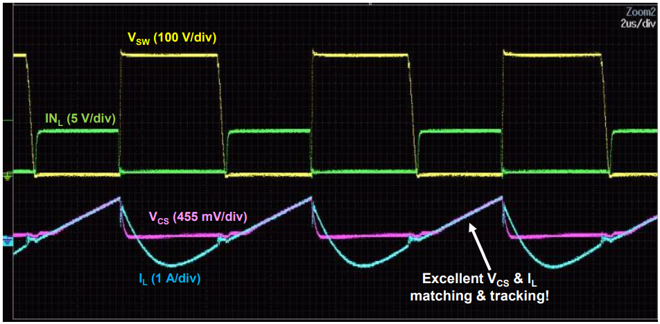
During bench testing, the switching waveforms (Fig. 9) show the CS pin tracking performance versus inductor current (IL). The switching performance shows excellent VCS and IL real-time matching and tracking at 1 A peak current levels for 120 W asymmetrical half-bridge (AHB) application circuit during steady-state, full-load ZVS conditions. To show tracking accuracy, the CS pin voltage scale for all waveforms is based on RCS gain calculation to match current probe scale
Figure 9: Loss-less current-sensing waveforms (asymmetrical half-bridge circuit, POUT = 120 W)
Over-Current Protection (OCP)
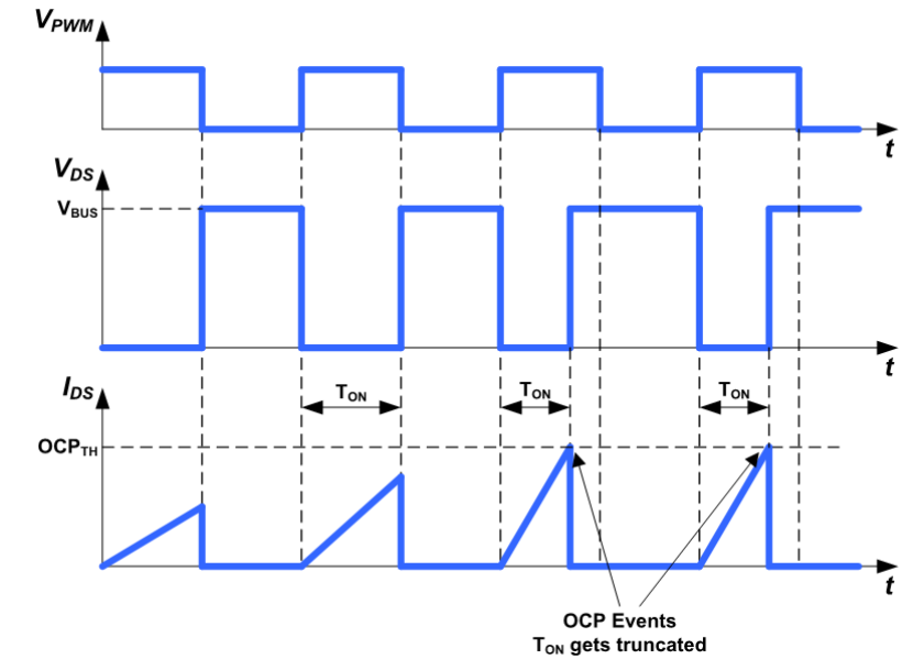
The IC includes cycle-by-cycle over-current detection and protection (OCP) circuitry to protect the lowside GaN power FET against high current levels. During the on-time of each low-side switching cycle (INH = low, INL = high), should the peak current exceed the internal OCP threshold (1.9 V, typical), then the internal low-side gate drive will turn the low-side GaN power FET off quickly and truncate the low-side on-time period to prevent damage from occurring to the IC. The IC will continue to function normally, and the high-side GaN power FET will then turn on at the next rising edge of the INH input pulse (Fig. 10) for the duration of the high-side on-time. After the high-side on-time period has ended, the low-side GaN power FET will turn on again at the rising edge of the next INL input pulse. Should the peak current exceed the OCP threshold again during the low-side on-time period, the OCP circuit will truncate the low-side on-time again. This cycle-by-cycle OCP protection feature will self-protect the IC each low-side switching period against fast peak over current events and greatly increase the robustness and reliability of the system. The OCP threshold equation (Equation 2) is a function of the internal current-sensing ratio and the external RSET resistor and can be used to program the desired OCP current limit level (IOCP). The internal OCP threshold (1.9 V, typical) is much higher than OCP thresholds of many popular PWM controllers. This ensures good compatibility of this IC with existing controllers without OCP threshold conflicts.

Figure 10: OCP timing diagram
Equation 2: NV6245C OCP current limit threshold vs RSET
Over-Temperature Protection (OTP)
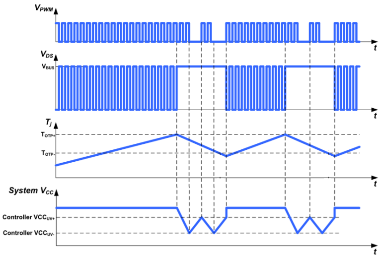
The IC includes over-temperature detection and protection (OTP) circuitry to protect the IC against excessively high junction temperatures (TJ). High junction temperatures can occur due to overload, high ambient temperatures, and/or poor thermal management. Should TJ exceed the internal TOTP+ threshold (165℃, typical) then the IC will latch off safely (Fig. 11). When TJ decreases again and falls below the internal TOTP threshold (105℃, typical), then the OTP latch will be reset. Until then, internal OTP latch is guaranteed to remain in the correct state while VCC is greater than 5 V. During an OTP event, the IC will latch off and the system VCC supply voltage can decrease due to the loss of the aux winding supply. The system VCC will fall below the lower UV- threshold of the system controller and the system high-voltage start-up circuit will turn-on and VCC will increase again (Fig. 10). VCC will increase above the rising UV+ threshold and the controller will turn on and deliver PWM pulses again, but the IC will remain off until TJ has decreased below TOTP- and the OTP fault latch is reset. Once the fault latch is reset, the IC will start switching again at the next PWM pulses from the controller.

Figure 11: OTP timing diagram
Programmable Turn-on dV/dt Control
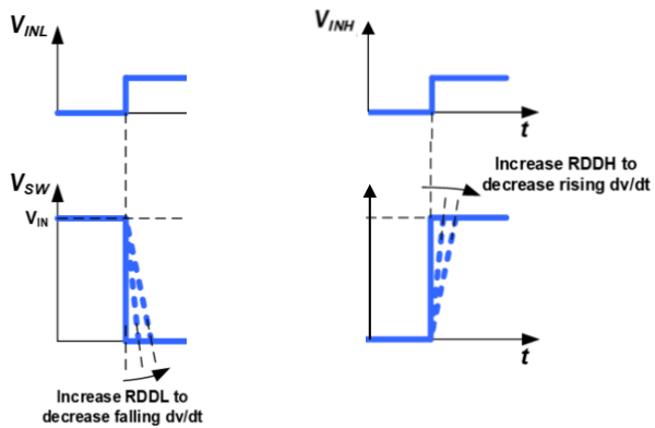
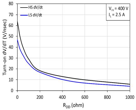
During first start-up pulses or during hard-switching conditions, it is desirable to limit the turn-on dV/dt slew rate of the drain of the low- or high-side GaN power FET. This is necessary to reduce EMI or reduce circuit switching noise. Resistor RDDL (pin 31) sets the turn-on current of the internal low-side gate driver and sets the turn-on dV/dt slew rate of the drain of the low-side GaN power FET (falling edge of the VSW node, Fig 12). Resistor RDDH (pin 23) sets the turn-on current of the internal high-side gate driver and sets the turn-on dV/dt slew rate of the drain of the high-side GaN power FET (rising edge of the VSW node, Fig. 12). The actual low-side and high-side turn-on dV/dt slew rates versus different RDDL/H resistor values are also shown (Fig. 13).
Figure 12: Turn-on dV/dt slew rate control timing diagram during hard-switching at low-side turnon (left) & hard-switching at high-side turn-on (right)
Figure 13: NV6245C graph for low-side turn-on slew rate dV/dt vs RDDL and high-side turn-on slew rate dV/dt vs RDDH
Programmable Turn-on dV/dt Control (Cont.)
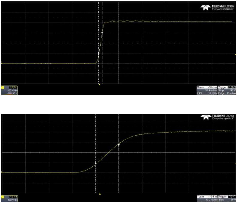
The high-side turn-on dV/dt slew rate control waveforms (Fig. 14) show the half-bridge switched-node voltage (VSW) for different RDDH resistor values. The waveforms exhibit very clean and smooth control for turn-on slewing at 10V/nsec and 75 V/nsec dV/dt rates. This simple programmability of turn-on speeds of both low- and high-side GaN power FETs using external resistors (RDDH and RDDL) allows for easy switching speed optimization and noise reduction. This is especially useful during conducted and radiated EMI compliance testing.
Figure 14: High-side turn-on dV/dt slew rate control waveforms, Vsw = yellow (100 V/div) Upper = 75 V/ns (RDDH =10 ohms), Lower = 10 V/nsec (RDDH = 1000 Ohms)
Programmable Turn-on dV/dt Control (Cont.)
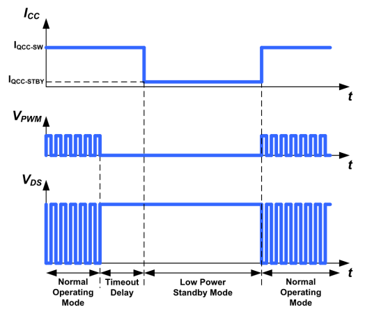
This GaNSense Half-Bridge IC includes an autonomous low power standby mode for disabling the IC and reducing the VCC current consumption. During normal operating mode, the PWM input signals at the INL and INH pins turn the gates of the internal high- and low-side GaN power FETs on and off at the desired duty-cycle, frequency, and dead-time. If the input pulses at the INL pin stop and stay below the lower VINLturn- off threshold (1.1V, typical) for the duration of the internal timeout standby delay (tTO_STBY, 90usec, typical), then the IC will automatically enter low power standby mode (Fig.15). This will disable the gate drive and other internal circuitry and reduce the VCC supply current to a low level (300uA, typical). When the INL pulses restart, the IC will wake up after a delay (typically around 490ns) at the first rising edge of the INL input and enter normal operating mode again. To enable auto standby mode, the STBYN pin should be connected to Source (set low). To disable auto standby mode, STBYN pin should be connected to the 5VL pin 7 (set high).

Figure 15: Autonomous low-power standby mode timing diagram
PCB Layout Guidelines (PQFN 6×8 mm)
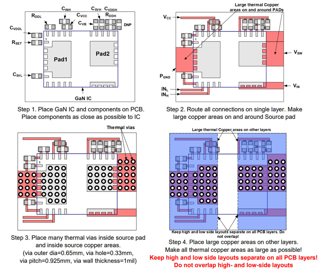
For best electrical and thermal results, these PCB layout guidelines (and 4 steps below) must be followed:
1) Place IC components as close as possible to the GaN IC. Place RSET resistor directly next to CS pin to minimize high frequency switching noise.
2) Connect the ground of IC components to Source to minimize high frequency switching noise. Connect controller ground also to Source (PGND).
3) Route all connections on single layer. This allows for large thermal copper areas on other layers.
4) Place large copper areas on and around Pad1 and Pad2.
5) Place many thermal vias inside Pad1 and Pad2 and inside Pad1 and Pad2 copper areas.
6) Place large possible copper areas on all other PCB layers (bottom, top, mid1, mid2).
Do not extend copper planes from the low-side across the components or pads of the high-side; do not extend copper planes from the high-side across the components or pads of the low-side! Keep high and low-side layouts separate. Do not overlap!

Figure 16: PCB layout steps
Electrical Simulation Model
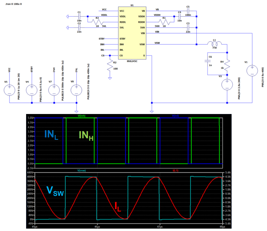
PSPICE-based electrical simulation models have been developed for the NV624x product family. This models are compatible with SiMetrix, LTSPICE and PSPICE platforms and include all internal circuitry and logic, current-sensing, level-shifting and both high- and low-side GaN power FETs. A typical LTSPICE simulation circuit and steady-state waveforms are shown for a ZVS resonant application circuit (Fig. 17). Both PWM inputs (INH and INL) are shown together with the half-bridge switched node (VSW) and output resonant inductor current (IL).
Figure 17: NV6245C electrical-simulation model & ZVS resonant circuit and simulation waveforms
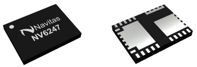
A 3D mechanical model has been developed for this IC (Fig. 18). The NV6247.stp file is available and easily importable into many popular PCB design software platforms (such as Altium Designer). This model is useful for generating 3D renderings of assembled power supply designs to check for any design issues before releasing PCB gerber files for manufacturing.
Figure 18: Top & bottom views of 3D mechanical model of NV624x (.stp file)
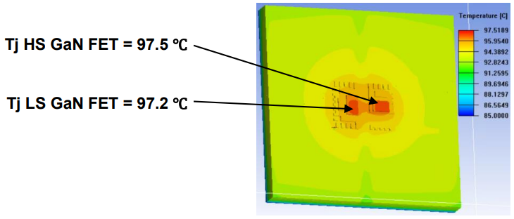
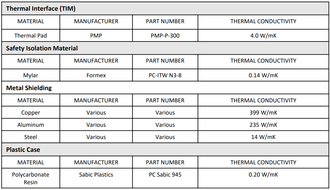
The following thermal model (Fig. 19) is for a PCB daughtercard with the IC mounted on one side of the PCB. The heat from the IC flows through the package leadframe, to the PCB copper layers and thermal vias, through the thermal interface material (TIM) and laterally through the PCB to the sides. The TIM then goes to the safety insulating material (Mylar) and then to a Cu shield (used for heatsinking and EMI suppression). The thermal conductivity for these materials are listed in Table III. To represent the actual thermal conditions inside a 140 W charger running at full load, the Cu shield is held at 85℃, the TAMB is set at 80℃, and PLOSS for both GaN power FETs is set at 1 W total. From the thermal simulation (Fig. 20), the TJ of the high-side GaN FET = 97.5℃ and Tj of the low-side GaN FET = 97.2℃. This result looks reasonable for the IC running during worst case line, load and ambient temperature conditions. Further improvement of the IC temperature is possible by using TIM with higher conductivity and by using thinner Mylar (if safety conditions allow).

Figure 19: Bottom-cooled thermal-model stack-up diagram
Figure 20: 3D thermal simulation results (PLOSS_HS GaN + LS GaN = 1 W, TAMB = 80℃)
Thermal Management (cont.)
Materials commonly used for shielding include copper or aluminum. Steel can be also be used for improved EMI shielding and is typically tin-plated to prevent rusting or corrosion. Some available thermal stack-up and shielding materials are summarized in the table below (Table 2).
Table 2: Thermal stack-up and shielding-materials summary.
References (www.navitassemi.com)
1) GaNFast NV6245C datasheet, Navitas Semiconductor, 2022
2) New GaNFast Power ICs with GaNSense Technology Loss-Less Current Sensing & Autonomous Protection, AN015, Navitas Semiconductor, 2021
3) Thermal Management of GaNFast Power ICs, AN010, Navitas Semiconductor, 2019

DISCLAIMER Navitas Semiconductor (Navitas) reserves the right to modify the products and/or specifications described herein at any time and at Navitas’ sole discretion. All information in this document, including descriptions of product features and performance, is subject to change without notice. Performance specifications and the operating parameters of the described products are determined in the independent state and are not guaranteed to perform the same way when installed in customer products. The information contained herein is provided without representation or warranty of any kind, whether express or implied. This document is presented only as a guide and does not convey any license under intellectual property rights of Navitas or any third parties. Navitas’ products are not intended for use in applications involving extreme environmental conditions or in life support systems. Terms and Conditions.
Navitas Semiconductor, Navitas, GaNFast, GaNSense and associated logos are registered trademarks of Navitas. Copyright ©2023 Navitas Semiconductor. All rights reserved Contact: [email protected]
![27_Pdf_File_Type_Adobe_logo_logos-512[1]](https://navitassemi.com/wp-content/uploads/2020/12/27_Pdf_File_Type_Adobe_logo_logos-5121.png)
