Gallium Nitride: Fast Forward to the GaN Data Center
![27_Pdf_File_Type_Adobe_logo_logos-512[1]](https://navitassemi.com/wp-content/uploads/2020/12/27_Pdf_File_Type_Adobe_logo_logos-5121.png)
Gallium Nitride: Fast Forward to the GaN Data Center
by Stephen Oliver
Gallium Nitride Speeds Past Silicon’s Limits
The ‘silicon chip’ has been the backbone – indeed the enabler – of the data revolution, both in terms of data processing in CPUs, GPUs, memory, networking, etc. and in terms of power conversion from high-voltage AC all the way down to the 1V needed by the microprocessor. The problem is that silicon as a power conversion platform has hit its physical limits and it’s time for a new semiconductor – gallium nitride (GaN) – to take its place. A worldwide Si-to-GaN data center upgrade would reduce energy loss by 30-40%, which would translate as saving over 100 TWh and 125 Mtons of CO2 emissions by 2030.
Consolidation of Data Centers – Hyperscale
As internet protocol (IP) traffic continues to rise, economies of scale mean that data centers are consolidating into ‘hyperscale’ operations (Fig. 1). These facilities are built from scratch, and therefore are not tied to legacy or retrofit power solutions.

Fig. 1) Annual IP traffic increases and the rise of the ‘hyperscale’ data center. i[Cisco]
Consolidation of Server and Telecom Architectures – HVDC
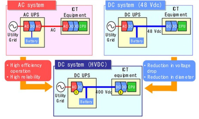
Let’s look at the architecture of a data center and where GaN can reduce loss, therefore save money and natural resources. For server, this is typically AC to 12 V in an air-conditioned room while for legacy, low-function (e.g. voice only) telecom systems this was the remote, damp ‘cell tower’ which needed AC to ‘anti-corrosion’, negative-referenced 48 V for battery back-up. As traffic increased, most telecom systems outgrew the original ‘cell-tower-only’ structure and are now in similar ‘clean’ environments, so the 48V can be positive-referenced and use similar system components as server. This trend is expected to continue as forecasts show a 30x increase in data traffic in only 10 years from 2015 to 2025. In the consolidated approach, we can also benefit from transition from ACdistribution to 400 V distribution approach as shown in Fig. 2.

Fig 2: The consolidation of server AC and telecom 48 VDC architectures into a 400 VDC HVDC system. [NTT]
Why Gallium Nitride?
Gallium (Ga, atomic number 31) and nitrogen (N, 7) combine into a semiconductor material – gallium nitride (GaN) – like Silicon (Si, 14). GaN is a ‘wide band-gap’ material because it offers an electron band-gap that is 3x larger than silicon, which means it can handle large electric fields with dramatically smaller chips. With much smaller transistors and shorter current paths, ultra-low resistance & capacitance is achieved, while enabling up to 100x faster switching speeds. Low resistance and low capacitance translate to higher power-conversion efficiencies, so more power is delivered to the IT load. This means more functions or ‘operations’ per Watt, instead of burning up that energy as heat which warms the system and creates additional cooling (air-conditioning) workload. In addition, high-speed (frequency) switching means smaller size & lower weight, as the energy-storing passive components can shrink dramatically as they store much less energy in each switching cycle.
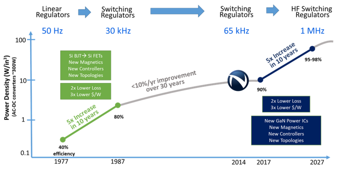
The practical and high-performance implementation of GaN as a power component building block is in an integrated solution – the GaNFast power IC from Navitas Semiconductor iv. Here, GaN power (FET), drive, control and protection are highly integrated to create an easy-to-use, high-performance, high-frequency (2 MHz), ‘digital-in, power-out’ building block. GaN power ICs are a catalyst to the second revolution in power electronicsv.

Fig. 3) Two revolutions in power electronics, with the ‘perfect storm’ of a new switch material, integration, new magnetics and new topologies making the transition from academia to industry. The result of each revolution being significant increases in switching frequency, efficiency power density and massive reduction in cost. The introduction of the GaN power ICs is indicated by the entry of Navitas Semiconductor in 2014. [Navitas]
The ‘second revolution’ started in the mobile fast-charger market with aftermarket accessory companies like Anker, AUKEY and Belkin offering single-port and multi-port GaN-based chargers from 30-100W. Tier-1 OEMs like Lenovo, Dell, Xiaomi, OPPO and Asus subsequently released smartphone and laptop chargers ranging up to 300W. Over 13 million GaNFast power ICs have now shipped with zero field failures and over 17 billion device field hours vi . This reliability data is a critical foundation for the adoption of gallium nitride by the conservative, ‘mission-critical’ data center market.
GaN with AC Input
For a traditional AC-in architecture, GaN can be employed in high-frequency, soft-switching topologiesvii . For the power factor correction (PFC) stage, the traditional hard-switching, low- frequency (47 kHz) boost is upgraded to a soft-switching MHz ‘totem-pole’, and the DC-DC stage upgraded in similar fashion. An example of an ‘all GaN’ 3.2 kW approach is shown in figure 4, with a MHz totem-pole PFC followed by MHz LLC. Navitas 650 V GaN is used for the PFC and DC-DC primary, with EPC 80 V GaN for the DC-DC secondary side rectification viii,ix . The design measures just 1U x 2U x 210 mm (800 cc) and achieves power density of 4 W/cc (65 W/in3 ).

Fig. 4) 3.2 kW AC-54V converter; 650V GaNFast power ICs for MHz totem-pole PFC and MHz LLC primary with 100V GaN FETs for LLC secondary rectification. [North Carolina State University and University of Texas, Austin]
In industry, Eltek (Delta Electronics) announced the 3 kW Flatpack2 SHE in 2017 x ; the first in a series of GaN-based AC-48/54/60 V power supplies which achieve 98% efficiency and a 50% reduction in loss vs. earlier silicon converters.
GaN with 400 VDC (HVDC) Input
For HVDC, the essential equation derived from Ohm’s Law is “Power loss = I2R” so for each distribution network or connector, maintaining as high a voltage as possible minimizes the current for a given power, and so reduces loss. The concept of HVDC in the data center is not new; with work by NTT back in 1999xi , and followed-up by Lawrence Berkley National Labs in 2006xii and Intel in 2007 xiii. However, the data center market is conservative, and change happens slowly. Adoption is being accelerated by factors like the cost of electricity (in $/kWhr), adherence to the ‘net-zero’ carbon emissions goal of the Paris Accord, and using new technology to amplify the advantages of architecture changes, i.e. Si-to-GaN.
For an HVDC network, we can use the post-PFC DC-DC ‘back-end’ of a traditional AC-48 VDC supplyxiv or turn to a more optimized, more granular approach where power can be converted in integers of 300 W (or similar) and be located at the closest point to the load(s) – thus maximizing the longest path at the highest voltagexv.
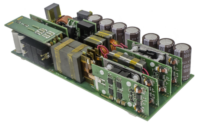
The advantage of GaN in such modular designs is clear when comparing the best-in-class silicon production designs (100 W), and silicon prototypes (300 W) which required stacked PCBs and large heatsinks. Figure 5 shows these silicon designs plus a new 400 V, 300 W, single-PCB design using NV6117 GaNFast power ICsxvi which follows the industry-standard ‘DOSA’ ¼-brick package and pin- out for simple installation and upgrade. Over a wide-range 330-425 V DC input, and from -40°C to +100°C operating temperature, the GaN converter delivers the full 300W in only 30 cc without derating. The means a world’s best-in-class power density of 10 W/cc, and 2x more power than any other mass-production DOSA-compliant high-voltage ¼-brick converter xvii. The current 300W design uses an industry-proven, hard-switched half-bridge topology at a record 400 kHz operating frequency, with efficiency as high as 94.5% at full load. With a soft-switching topology, over 1 MHz can be achieved with further power density target of 1 kW in a ¼-brick.

Fig. 5) 400 V ¼-brick designs: The single-PCB GaN design using Navitas NV6117 GaNFast power ICs has 2x the power density (W/cc) of any Si-based converter. [Navitas]
GaN from 48 V to the Load
For the lower-voltage distribution network, an upgrade from 12 V to 48 V means a 16x reduction in distribution loss. This change was pioneered by companies like IBM in the Blue Gene/P supercomputer in 2007 and by Google for their Hong Kong data center in 2014. As the power needed for GPUs has increased, NVIDIA have also switched their GPU-module input rail from 12 V to 48 V – a change that has been extended to high-end laptops, with a matching 300 W AC-48V adapter using GaNFast power ICs xviii.
From ~48 V down to the CPU, GPU and memory, low-voltage GaN (<=80 V) can be deployed. For a 48 V – 6 V down conversion, GaN achieves 300 W from a 27 x 18 mm open-frame DCX (LLC) at over 100 W/cc (1700 W/in3)xix . Getting to the processor voltages (as low as 0.6V at over 100A) requires new topologies from 48V-1.xV, or adopting new fully-integrated voltage regulator ‘FIVR’ topologies pioneered by the Intel Haswell processorxx and advanced in similar fashion by highly-integrated, high-frequency solutions like the Empower IVRxxi.
GaN Takes Over
As data center traffic accelerates, silicon’s ability to process power effectively and efficiently hits ‘physical material’ roadblocks and the old, slow, silicon chip is overtaken by high-speed gallium nitride. The consolidation of data center hardware, a new HVDC architecture approach and the proven reliability of mass-production, highly-integrated GaN power ICs enable major improvements in efficiency. This ‘fast-forward’ means another step towards carbon ‘Net-Zero’ goals for the whole power electronics and data center industries.
References (www.navitassemi.com)
i Cisco Global Cloud Index: Forecast and Methodology, 2016–2021 (2018): https://www.cisco.com/c/en/us/solutions/executive-perspectives/annual-internet-report/index.html
ii Ericsson Mobile data traffic outlook https://www.ericsson.com/en/mobility-report#:~:text=Global%20total%20mobile%20data%20traffic,164EB%20per%20month%20in%20202
iii A. Matsumoto, A. Fukui, T. Takeda and M. Yamasaki, “Development of 400-Vdc output rectifier for 400-Vdc power distribution system in telecom sites and data centers,” Intelec 2010, Orlando, FL, 2010, pp. 1-6, doi: 10.1109/INTLEC.2010.5525652.
iv D.Kinzer and S. Oliver, “Monolithic HV GaN Power ICs: Performance and application,” in IEEE Power Electronics Magazine, vol. 3, no. 3, pp. 14-21, Sept. 2016, doi: 10.1109/MPEL.2016.2585474.
v “Oliver, Xue, Huang, “From Science Fiction to Industry Fact: GaN Power ICs Enable thev “Oliver, Xue, Huang, “From Science Fiction to Industry Fact: GaN Power ICs Enable theNew Revolution in Power Electronics”, Bodo’s Power Magazine, Dec. 2017 https://navitassemi.com/download/from-science-fiction-to-industry-fact-gan-power-ics-enable-the-new-revolution-in-power-electronics/?wpdmdl=37063&ind=1562849999810
vi “Navitas Ships 13,000,000 GaNFast Power ICs with World-Class Reliability”, Navitas, January 2021 https://navitassemi.com/navitas-ships-13000000-ganfast-power-ics-with-world-class-reliability/
vii Kinzer, “Driving for Zero Losses”, PCIM Asia, Navitas, June 2016 https://navitassemi.com/download/driving-for-zero-switching-losses/?wpdmdl=36519&ind=1561099847555
viii Huang, et al, “Adaptive Zero-Voltage-Switching Control and Hybrid Current Control for High Efficiency GaN-Based MHz Totem-Pole PFC Rectifier”, NCSU, Navitas, APEC 2017
ix R. Yu, Q. Huang, T. Chen, A. Q. Huang and T. Ribarich, “High-Frequency and High-Density Design of all GaN Power Supply Unit,” PCIM Europe 2018; International Exhibition and Conference for Power Electronics, Intelligent Motion, Renewable Energy and Energy Management, Nuremberg, Germany, 2018, pp. 1-5. https://ieeexplore.ieee.org/document/8402908
x Eltek launches the Flatpack2 SHE, a Super High Efficiency power conversion module with the new CoolGaN™ technology from Infineon at its core” October 2017 https://www.eltek.com/us/insights/eltek-launches-the-flatpack2-she-a-super-high-efficiency-power-conversion-module-with-the-new-game-changing-coolgan-technology-from-infineon-at-its-core/
xi T. Yamashita, et al., “270 V DC – A Highly Efficient and Reliable Power Supply System for Both Telecom and Datacom Systems,” IEEE Intelec ‘99, Copenhagen, 1999.
xii M. Ton et al., “High Performance Buildings: DC Power for Improved Data Center Efficiency”, Lawrence Berkeley National Laboratory, December 2006
xiii A. Pratt, P. Kumar and T. V. Aldridge, “Evaluation of 400V DC distribution in telco and data centers to improve energy efficiency,” INTELEC 07 – 29th International Telecommunications Energy Conference, Rome, Italy, 2007, pp. 32-39, doi: 10.1109/INTLEC.2007.4448733. https://ieeexplore.ieee.org/document/4448733
xiv N. Hanaoka, A. Takahashi, T. Tanaka, N. Yamashita and M. Sugahara, “Development of high-efficiency downsized power conversion (380 V to −48 V) equipment for HVDC power supply system,” 2015 IEEE International Telecommunications Energy Conference (INTELEC), Osaka, 2015, pp. 1-6, doi: 10.1109/INTLEC.2015.7572361. https://ieeexplore.ieee.org/document/7572361
xv iNEMI 380-12V DC-DC Power Module project, https://community.inemi.org/content.asp?contentid=424
xvi https://navitassemi.com/technology/
xvii “Density Power 300W https://navitassemi.com/navitas-delivers-2x-more-power-for-industrial-telecom-and-data-center-power-supplies/
xviii Asus/NVIDIA Pro Art uses 300W AC-48V adapter. Navitas PR: https://navitassemi.com/navitas-enables-worlds-smallest-adapter-for-worlds-fastest-laptop/
xix EPC 48V reference designs https://epc-co.com/epc/Applications/DC-DCConversion/GaN-in-High-Density-Servers-ebooklet.aspx?utm_source=LinkedIn&utm_medium=Post&utm_campaign=MPS%2048V&utm_content=DC7
xx Prototype Haswell processor demonstrated at the Intel Developer Forum 2013 https://en.wikipedia.org/wiki/Haswell_(microarchitecture)
xxi Empower IVR https://www.empowersemi.com/technology/


GaN, GaNFast and the GaNMan are all copyright Navitas Semiconductor Ltd 2021.
22 Fitzwilliam Square South, Saint Peter’s, Dublin, D02 FH68, Republic of Ireland
www.navitassemi.com
www.ganfast.com
Tel.: ThinkGaNIC +1 (844-654-2642) [email protected]