Gallium Nitride (GaN) Power ICs: Turning Academic Dreams into Industry Reality
This article was featured in Bodo’s Power Systems (May 2021)
![27_Pdf_File_Type_Adobe_logo_logos-512[1]](https://navitassemi.com/wp-content/uploads/2020/12/27_Pdf_File_Type_Adobe_logo_logos-5121.png)
Gallium Nitride (GaN) Power ICs: Turning Academic Dreams
into Industry Reality
Gallium nitride (GaN) is the key enabler for high-frequency, and simultaneously
high-efficiency topologies.
by Stephen Oliver and Tom Ribarich
Like Leonardo da Vinci (1452-1519) and his amazing inventions, including the ‘helicopter’ and ‘robotic knight’, electronics academics have long been frustrated that their ideas cannot become reality due to the limited materials available at the time. Leonardo would be amazed at today’s lightweight alloys and tiny, high-speed electric stepper motors compared to his rudimentary ironwork and waterpower. Now, old, slow, lossy silicon chips are consigned to history, as new, fast, efficient gallium nitride (GaN) power ICs turn academic dreams into industrial reality from mobile fast chargers to data center power supplies.

Gallium Nitridei : High-Speed Enabler
High-speed – or rather – high-frequency power topologies mean smaller and smaller passive components, to the extreme case that in a 40 MHz phi-2 converter at Stanford Universityii, the ferrite material completely disappears in an ‘air-core’ inductor.
The flyback converter has had several proposed improvements, such as the high-frequency quasi-resonant (HFQR) from Professor Fred Lee at Virginia Polytechnic (VPT) in 1988iii, and R. Watson’s active-clamp flyback (ACF), also from VPT in 1996ivwhich eliminated snubber loss. However, in each case, the output capacitance (COSS) of the silicon MOSFET created such high switching lossesv that implementation was not feasible – so no commercial control ICs would be financially viable.
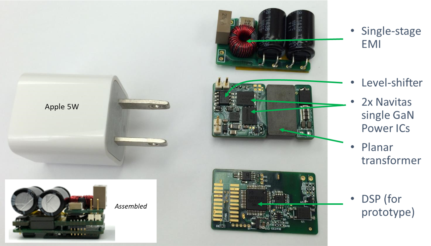
Twenty years later, in 2016, a prototype 25 Wvi ACF switching at 1 MHz was designed by Xiucheng Huang at VPT using Navitas GaNFast power ICs and a TI DSP controller (C2000). Further MHz work using a GaNFast half-bridge power IC was completed at Zhejiang University in 2019vii. Though tiny designs, the DSP is designed for high-power industrial applications, and has a relatively high leakage current. As a result, the designs couldn’t meet US DoE Level VIviii low-power standby requirements – in effect from February 2016 – so were not commercially practical.
GaNFast power ICs were the enabler for high-frequency systems, based on a) GaN’s physical advantages over silicon, and b) robustix performance and ease-of-use resulting from monolithic integration of GaN power (FET) and driver, plus protection and control. Since mass production release, GaNFast power ICs have been rated at 2 MHz which is 20x faster than typical converter switching frequency of 50-60 kHz.

Figure 1: Left: High-performance, high-frequency 1 MHz 25 W activeclamp flyback (ACF) prototype from CPES (Virginia Polytechnic), using Navitas gallium nitride (GaN) power ICs, planar transformer and C2000 DSP. Prototype achieved 17 W/in3 (estimate, cased).
A reliable, high-performance, high-speed GaN powertrain meant that control IC companies could confidently invest time and resources to design and release speed-optimized ASICs which met DoE Level VI requirements and be part of cost-effective system bills of material (BoMs). The first Level VI-compatible high-frequency controller was the TI UCC28780 with a headline peak frequency of 1 MHz for ACF, which was used in the world’s first, and thinnest 45W USB-C fast charger – the Mu Onex. This was quickly followed by the HFQR NCP1342 from On Semi, which increased switching frequency 4x from 50 kHz to 200 kHz, ending a frustrating 30-year wait.
A recent upgrade to ACF has been the ‘Pulsed-ACF’xi, as used in OPPO’s 50W Mini “Cookie” charger, which achieves another ‘vanishing act’. The electrolytic ‘bulk cap’ can occupy 40% of the total charger size but a proprietary innovation creates the world’s first charger using ‘pulsed’ power conversion. This eliminates the electrolytic bulk capacitor, and the rectified 100 Hz pulsating DC feeds directly into the high-frequency ACF circuit which can maintain a smooth output to charge the phone’s battery, even when the input voltage range is wide. A follow-on benefit is that OPPO-proprietary ‘direct-charge’ approach means that during each pulse gap, the polarization effect in the phone battery is eliminated so reducing wear-out mechanisms and extending battery life.

Figure 2: OPPO 50W Mini “Cookie” charger, showing high-frequency planar magnetics and elimination of electrolytic bulk capacitor.
Higher Power, Higher Speeds
As we move to higher powers (>75W), power factor correction (PFC) is required, and we also face the perennial problem of the lossy diode bridge rectifier.
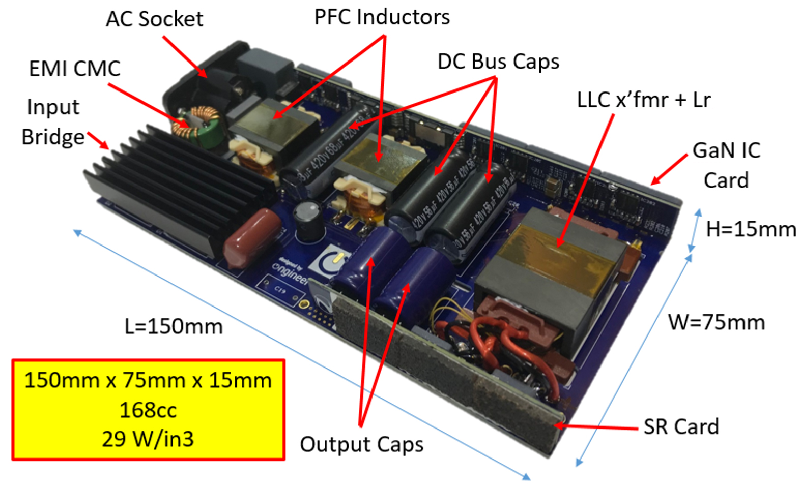
Traditional PFC has been constant current (CCM) or discontinuous conduction mode (DCM) boost with a main switch and diode. GaN’s wide band-gap sibling – silicon carbide (SiC) – has helped to minimize diode drop and reverse-recovery losses. However, silicon’s switching losses (specifically COSS) continued to limit frequency to around 50-60 kHzxii. In a similar story to the ACF, the introduction of GaN power ICs spurred new PWM controllers. One example chip-set was the NCP1631 interleaved CrCM boost, NCP13992 LLC, and NCP4305/43080 SR PWM controllers as used in the world’s smallest 300W reference design by Ongineerxiii. This was the inspiration for the Asus / NVIDIA AC-48V 300 W laptop charger using GaN power ICsxiv.

Figure 3: 300 W AC-19 VDC reference design using GaN power ICs: Interleaved CrCM/DCM Boost using NCP1632 (with frequency-foldback function to reduce power consumption), minimum 200 kHz (90 VAC, peak-of-line) to maximum 450 kHz. LLC using NCP13992 (with adaptive dead-time features, soft-start, comprehensive protection and HV start-up) and NCP4305/NCP43080 (SR), 500 kHz normal operation (with higher frequency during load / start-up burst conditions).
The next architectural advance was the ‘bridge-less’ boost PFC from Milan Jovanovicxv which combined the AC bridge rectifier plus PFC circuit, and used two switches for AC-rectification and two more switches for the PFC function. This was described in 2008 and was used in high-power server AC-48V and AC-12V power supplies but remained low-frequency due to hard-switching silicon FETs, so had a small increase in efficiency but no change in power density. A later development was the ‘totem-pole’ variantxvi but still only 50 kHz. With gallium nitride, the frequency-related limits of silicon are overcome, and high-frequency CrCM ‘totem-pole’ PFC becomes a reality.
For a 300 W laptop adapter, the upgrade from AC-bridge plus 50 kHz boost PFC, to 200-500 kHz CrCM totem-pole using a new Level VI-compliant PWM controller and new GaN power ICs like the NV6128xvii achieves power density over 1.1 W/cc. This is 3x smaller and lighter than current tier-1 OEM designs.
Moving up in power and frequency, a prototype 3.2 kW AC-54 V data center power supply was built at the University of Texas, Austin using a 100% gallium nitride powertrain with an interleaved CrCM totempole PFC running from 350 kHz to 1.5 MHz (sweep using CrCM).xviii 650 V GaN power ICs were used on all legs of the totem-pole and primary LLC, with 80 V GaN FETs on the secondary rectification side. Both PFC and DC-DC stages used planar magnetics and the C2000 DSP for control. As a data center SMPS is not classified as an ‘external supply’, the Level VI standby loss requirement does apply so in this case, the PWM controller was ready, waiting for gallium nitride to fulfill the academic’s needs, achieving 4.4 W/cc (73 W/in3).
Gallium Nitride: Living the Dream
Even in the renaissance period, the rate of technological innovation could not keep up with Leonardo’s dreams. Today, gallium nitride – in the form of the GaN power IC – delivers efficient, high-speed performance that has ended decades-long frustration; to fulfill academics’ dreams and advance them to industry-proven realities.
i “Gallium nitride”, https://navitassemi.com/gallium-nitridethe-next-generation-of-power/
ii Kinzer. “Breaking Speed Limits with GaN Power ICs”, APEC 2016 Keynote, https://navitassemi.com/articles/
iii F. C. Lee, “High-frequency quasi-resonant converter technologies,” in Proceedings of the IEEE, vol. 76, no. 4, pp. 377-390, April 1988, doi: 10.1109/5.4424. https://ieeexplore.ieee.org/document/4424
iv R. Watson, F. C. Lee and G. C. Hua, “Utilization of an activeclamp circuit to achieve soft switching in flyback converters,” in IEEE Transactions on Power Electronics, vol. 11, no. 1, pp. 162- 169, Jan. 1996, doi: 10.1109/63.484429.
v D. Kinzer, Navitas “Welcome to the Post-Silicon World: Wide Bandgap Powers Ahead”, keynote PCIM 2016.
vi S. Oliver, T. Ribarich, “State-of-the-Art Mobile Charging: Topologies, Technologies and Performance”, APEC 2017, Industrial Session IS05, https://navitassemi.com/articles/
vii D. Gu, J. Xi and L. He, “A Digital PWM Controller of MHz Active Clamp Flyback with GaN Devices for AC-DC Adapter,” IECON 2019, doi: 10.1109/IECON.2019.8927336. https://ieeexplore. ieee.org/document/8927336
viii “Efficiency standards for external power supplies” [Level VI]. CUI, https://www.cui.com/efficiency-standards
ix N. Fichtenbaum, “GaN Integrated Circuits for Power Electronics,” 2019 Device Research Conference (DRC), doi: 10.1109/ DRC46940.2019.9046333. https://navitassemi.com/articles/
x “Navitas’ GaNFast™ Enables World’s Thinnest Travel Adapter”, Navitas press release, March 2018, https://www.navitassemi. com/navitas-ganfast-enables-worlds-thinnest-travel-adapter/
xi “GaNFast Power ICs Enable OPPO’s 50W Mini ‘Cookie’ – the World’s Smallest, Thinnest Fast Charger”, Navitas press release August 2020, https://navitassemi.com/ganfast-power-icsenable-oppos-50w-mini-cookie-the-worlds-smallest-thinnest-fastcharger/
xii Gallium Nitride (GaN) output capacitance (COSS) is 20c lower than silicon at <30 V VDS. D. Kinzer, Navitas “Welcome to the Post-Silicon World: Wide Bandgap Powers Ahead”, keynote PCIM 2016.
xiii T. Ribarich, P. Bredemeier and S. Oliver, “GaN High Density 300W AC-DC Converter,” PCIM Europe 2019. Paper at https:// ieeexplore.ieee.org/document/8767722 , poster at https://www. navitassemi.com/articles/
xiv “Navitas Enables World’s Smallest Adapter for World’s Fastest Laptop”, Navitas press release, October 2019, https://www. navitassemi.com/navitas-enables-worlds-smallest-adapter-forworlds-fastest-laptop
xv L. Huber, Y. Jang, and M. M. Jovanović, “Performance evaluation of bridgeless PFC boost rectifiers,” IEEE Trans. Power Electron., vol. 23, no. 3, pp. 1381-1390, May 2008. https://ieeexplore.ieee. org/document/4483680
xvi B. Su and Z. Lu, “An Interleaved Totem-Pole Boost Bridgeless Rectifier, etc.” IEEE Trans. on Power Elec., vol. 25, June 2010, doi: 10.1109/TPEL.2010.2040633. https://ieeexplore.ieee.org/ document/5393032
xvii NV6128 650/800V gallium nitride (GaNFast) power IC: https:// www.navitassemi.com/download/
xviii Yu et al, “Monolithic GaN Power ICs Enable High Density High Frequency 3.2 KW AC-DC Rectifier,” PCIM Europe 2018; Nuremberg, Germany, pp. 1-4. https://ieeexplore.ieee.org/document/8402956


GaN, GaNFast and the GaNMan are all copyright Navitas Semiconductor Ltd 2021.
22 Fitzwilliam Square South, Saint Peter’s, Dublin, D02 FH68, Republic of Ireland
www.navitassemi.com
www.ganfast.com
Tel.: ThinkGaNIC +1 (844-654-2642) [email protected]
