Navitas GaNFast™ IC Field Results in High-Volume Production
![27_Pdf_File_Type_Adobe_logo_logos-512[1]](https://navitassemi.com/wp-content/uploads/2020/12/27_Pdf_File_Type_Adobe_logo_logos-5121.png)
Application-Specific Reliability Methods Drive Successful Navitas GaNFast™ IC Field Results in High-Volume Production
By Anthony Schiro, VP Quality & Sustainability, and Llew Vaughan-Edmunds, Senior Marketing Director
Successful implementation of a new semiconductor technology requires a robust, application-specific approach to technology validation, product validation and lifetime modeling
Quality is paramount when introducing an innovative technology and device family into mass production. Establishing robust design rules and understanding intrinsic failure modes is key to exceeding customer performance and reliability expectations in high-volume manufacturing. Since Navitas was formed in 2014, its GaNFast™ power ICs are now proven in the field for the highest reliability and performance, with over 210 billion field hours, over 50,000,000 units shipped, and zero GaN-related field failures observedi. Additionally, Navitas offers a 20-year limited warranty for its GaNFast technology – 10x longer than typical silicon, SiC or discrete GaN power semiconductors. This success comes from several key factors in Navitas’ strategic leadership in GaN power.
Most of today’s power semiconductors are based on silicon, which originates from a single crystal ingot created using a CZ (Czochralski), MCZ (magnetic field applied Czochralski), or Float Zone (FZ) crystalgrowth process. This monocrystalline lattice is then doped with boron or phosphorous to create an ntype or p-type semiconductor. GaN is different. It is a compound semiconductor that combines two elements (gallium and nitrogen), from groups III and V in the periodic table, forming a wide bandgap semiconductor. Creating a GaN crystal involves a completely different process than silicon, typically with a metal organic chemical vapor deposition (MOCVD) growth process.
Compound semiconductors behave differently to silicon and, therefore, have different physics-of-failure drivers in reliability. In 2016, the first working group of industry experts formed the GaN Standards for Power Electronic Conversion (GaNSPEC) Devices Working Group (DWG), to develop specific and credible standards for GaN power devices. Navitas was a key founding member and has collaborated to introduce guidelines for test methods, datasheet ratings and reliability testing. This was the basis of JEDEC’s subsequent JC-70 committee: JC-70 Wide Bandgap Power Electronic Conversion Semiconductors. The key outcome of the reliability testing committee has been broad agreement on the need for switching based stress testing in the reliability regime.
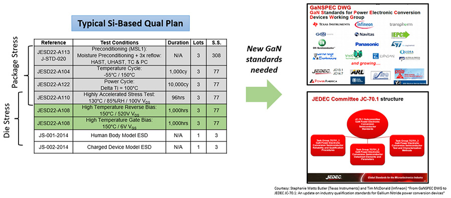
Figure 1: Navitas was a key founding member of GaNSPEC and JEDEC 70.1, focused on standards for GaN power devices.
Navitas’ Approach to Reliability
The Navitas approach to reliability is multi-faceted with an extensive quality and reliability methodology to demonstrate GaN as more reliable than its Si predecessor. Technology, design and manufacturing process choices are paramount to designing in quality and reliability from the start. Reliable products require robust design rules and characterization. Navitas’ AllGaN™ proprietary process design kit (PDK) is the result of years of studying, improving, and optimizing Power FET and IC device performance and reliability. Each element is evaluated independently and screened for defects and robust, stable parametrics.
Application-specific testing is critical to understand how the device performs in target applications under various conditions. The application-specific reliability approach is essential in new technology assessment since it is common to see high field failure rates in new technologies that simply retain legacy reliability test regimes such as high-temperature reverse bias (HTRB) and high-temperature gate bias (HTGB) for discrete power semiconductors. Combining application-specific testing with a test-tofailure approach is also important to identify key technology limitations and failure modes to drive improvements prior to technology and product release. Devices are assessed at expected and significantly accelerated application voltages, temperatures, and frequencies to develop acceleration factors and lifetime models in addition to standard reliability validation. While other GaN companies have experienced field reliability issues, Navitas’ application-specific test approach has proven successful with no field reliability concerns found in more than 50 million GaNFast ICs shipped in over four years since production release.
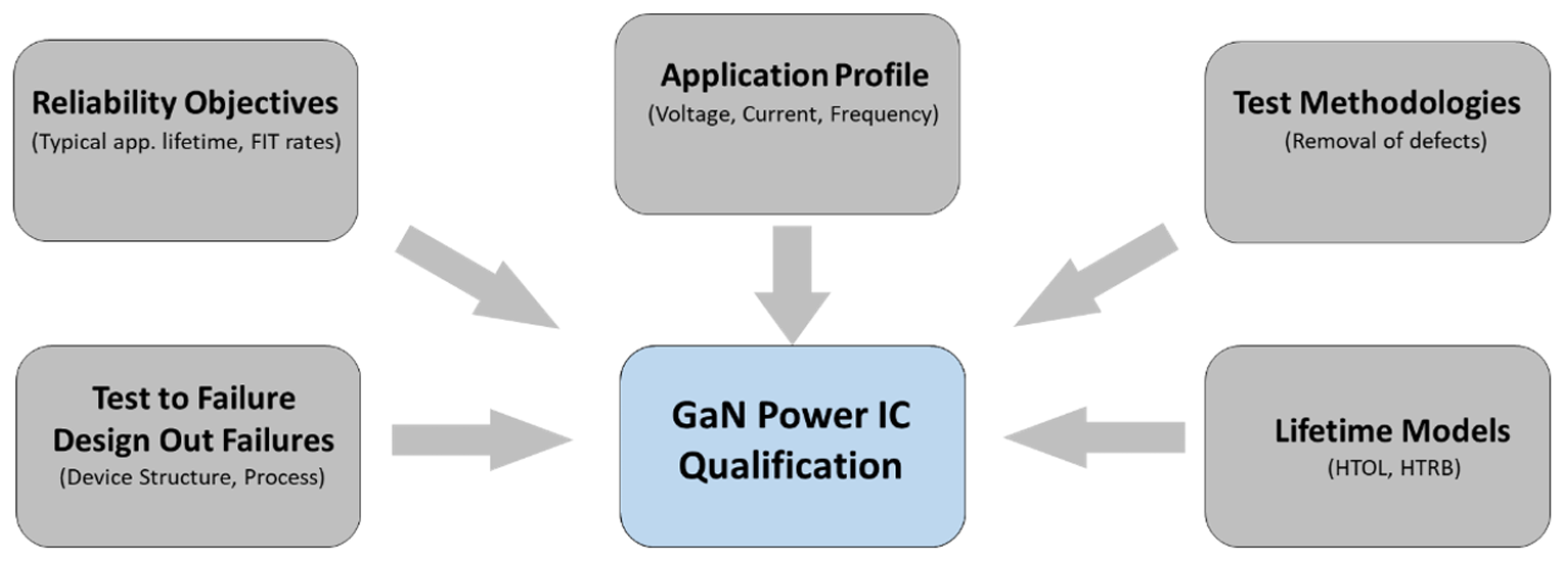
Figure 2: Many factors ensure Navitas GaN reliability.
Dynamic Testing
GaN power switches are high-electron-mobility transistors (HEMTs) with exceptionally low capacitances. Because they switch extremely quickly, dynamic testing is critical. JEDEC provides general guidelines for switching reliability evaluation procedures for GaN devices (JEP180), including dynamic high-temperature operating life (DTHOL), based on Navitas’ original research. Dynamic testing is critical to understand the true reliability in the application. Navitas exceeds the guidelines for dynamic testing with proprietary in-house-designed test methods to ensure the highest quality and reliability covering soft switching, hard switching, integrated driver switching, and surge voltage testing. Additional testing is conducted under dynamic application conditions, which provides better and more confident reliability prediction, as well as a broader system reliability than discrete component evaluation.
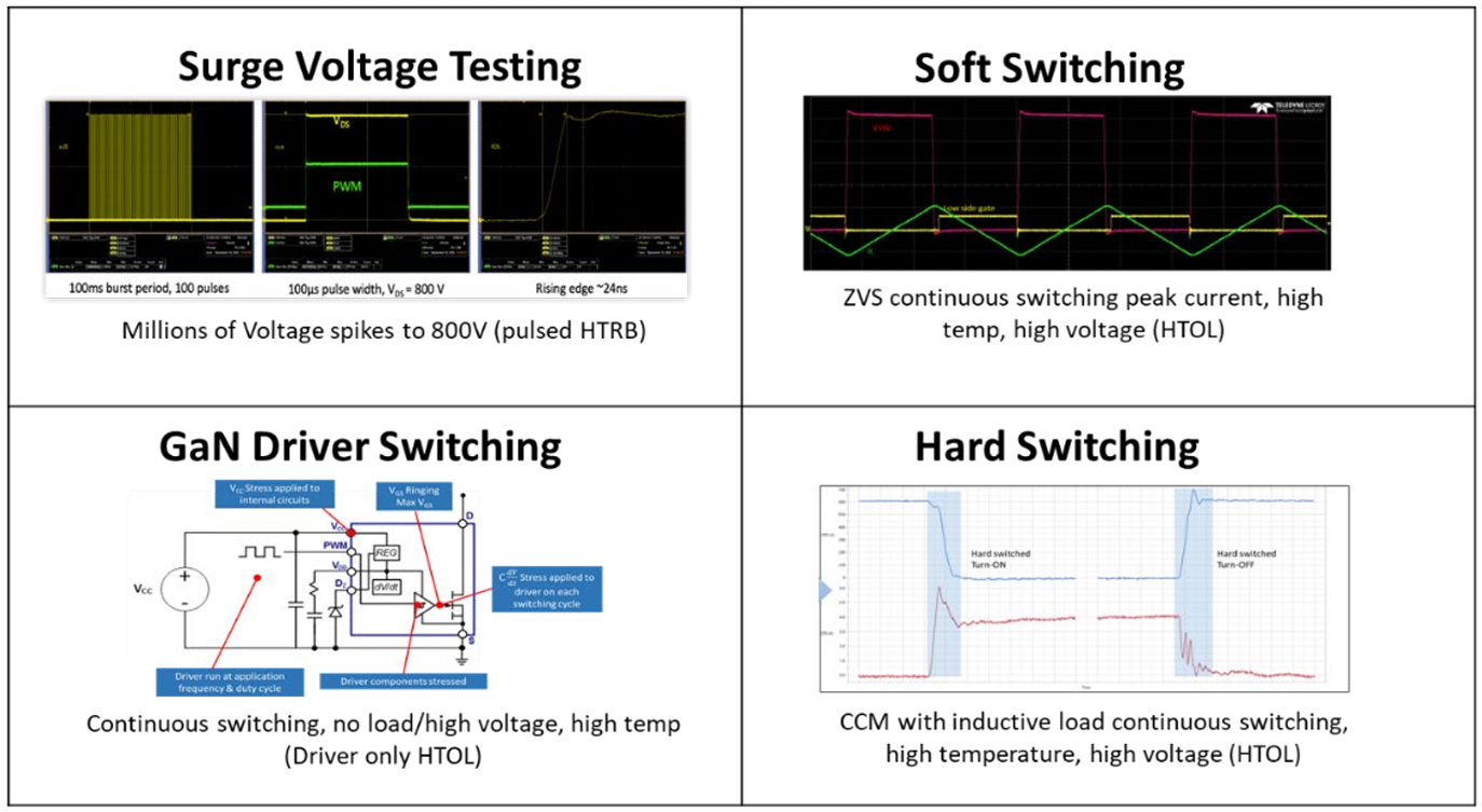
Figure 3: Navitas proprietary reliability methods ensure higher quality and more confidence in reliability prediction modelling.
Application-Specific Testing
One example of Navitas’ application testing is the high-temperature operating life – zero-voltage switching (HTOL-ZVS) test. This test has been used while targeting the mobile charging market and is relevant for many soft switching applications. Understanding each use profile at the system- and device-level identifies the key variables stressing the device and which reliability tests and test conditions are the most important.
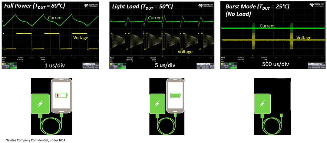
Figure 4: Application profiles for an active clamp flyback (ACF) charger with different stresses on the power device.
During burst profile (no load), the stresses seen on the GaN FET are relatively low. The operating junction temperature is low, switching frequency is low, and the current is minimal. However, the blocking voltage is high. From a reliability standpoint, HTRB testing is the key indicator to identify relevant stresses in this condition. During a full-load profile, the GaN FET exhibits high stresses. The junction temperature is at its highest, switching frequency is at maximum with high and fast transitions of voltage and currents. The HTOL-ZVS test provides an accurate test bench to study and validate device reliability over time in this condition.
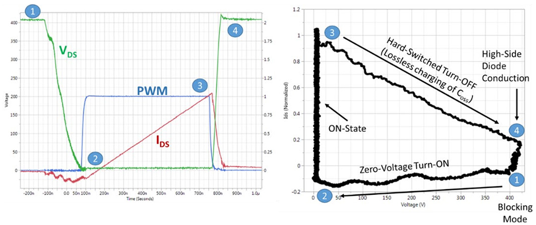
Figure 5: ZVS application profile (FET). ‘Soft switching’ or ZVS (zero voltage Switching) represents an application-relevant stress on the power FET.
Lifetime Modelling
Lifetime analysis is conducted at both the device and system level to determine the end-of-life (EOL) estimation based on the studied and expected failure mechanism. Accelerated HTOL-ZVS and HTRB tests are used to simulate system operating conditions and match all elements of application profiles. Testing is conducted to statistical sample sizes with test-to-failure data and varied conditions, to develop lifetime and acceleration models.
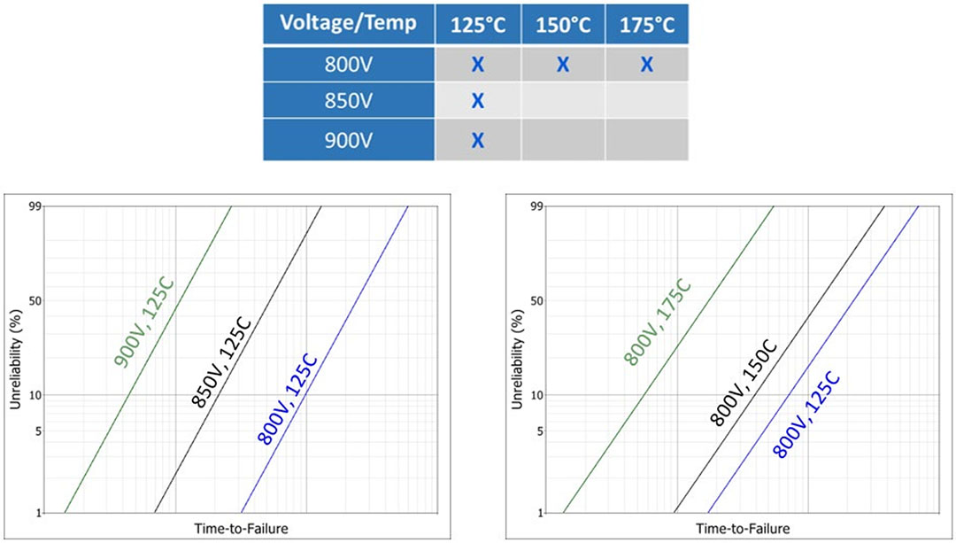
Figure 6: Accelerated test-to-failure determines reliability acceleration factors for voltage and temperature.
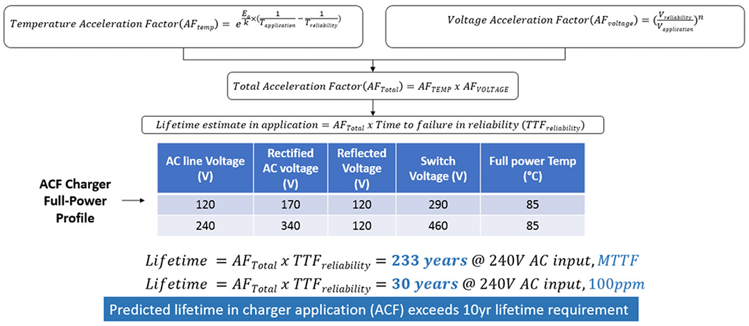
Figure 7: Lifetime estimation in charger application at full-power profile far exceeds expected 3-5 year lifetime requirement.
Production Monitoring
Navitas has constantly monitored all its high-volume production over the last four years with both standard test methods and application-specific test methods. This testing covers over 70 different fab lots and over 7000 parts-on-test, resulting in the highest possible confidence in the consistent reliability of GaNFast ICs. The results demonstrate a failures-in-time (FIT) rate – where 1 FIT equals one device failure in every 1 billion hours – that is six times better than silicon’s typically accepted value, positioning GaNFast ICs as a superior quality to silicon equivalents.

Figure 8: L Reliability monitoring of production material throughout three years of production tests – 7,276 units on high-frequency, soft-switching application-focused stress testing from over 70 fab lots.
Summary
Navitas’ commitment to new and innovative methods to validate the reliability of GaNFast ICs has paid off with field performance aligned to internal reliability data. With over 50,000,000 units shipped, 210 billion field hours, and zero GaN-related field failures, GaNFast power ICs are a proven technology in high-volume production.
Navitas’ focus on validating all the building blocks of the technology, ensuring robust design and materials choices and choosing an application-specific reliability validation regime have led to an excellent market introduction. A strong commitment to ongoing reliability monitoring in high-volume production provides a closed-loop approach of continuous product and technology improvements that feeds back into the design and development process, as the company continues to work on technology advancements, new technologies and address new, high-power markets to disrupt the power semiconductor world.