Step Up to Half-Bridge GaN Power ICs
![27_Pdf_File_Type_Adobe_logo_logos-512[1]](https://navitassemi.com/wp-content/uploads/2020/12/27_Pdf_File_Type_Adobe_logo_logos-5121.png)
Step Up to Half-Bridge GaN Power ICs
Half-bridge circuits are essential building blocks in the power electronics industry, used in everything from smartphone chargers and laptop adapters, to TVs, solar inverters, data centers and electric vehicles.
By Santosh Sharma, Dan Kinzer, Jason Zhang, Marco Giandalia, Stephen Oliver, Navitas Semiconductor
The Ubiquitous Challenge
Operating these half-bridge circuits – i.e. providing power and signal to a floating high-side switch – at very high frequencies can shrink magnetics and enable a dramatic reduction in size, cost and weight while delivering faster charging. However, such frequency increases have eluded the industry for decades as silicon devices have been too slow and suffer from parasitic impedances between the driver, high-capacitance silicon FETs and poorly performing level-shifter / isolators. As a result, most converters still run at 65-100 kHz. From the original opto-couplers, we have seen the introduction of hybrid-technology level shifters (capacitive coupling, inductive coupling) which enabled somewhat higher frequencies but are expensive and inefficient. Finally, lateral monolithically-integrated half-bridge Gallium Nitride (GaN) Power ICs have been introduced to enable a 30x increase in switching frequency.

Scope: Power and Topologies
The focus of this article is on half-bridge applications (Figure 1) with power levels from 20 W to 300 W+, and where 650 V functional (not galvanic) isolation is required to separate the ground-referenced control IC PWM signals from the high-side gate, and allows a switching node typically between 0 V and 400 V bus rail. Extended power range can achieved by the use of full-bridge circuits and interleaving half-bridges. In topology terms, and for high switching frequency, this includes softswitching circuits such as active clamp flyback (ACF) (20 W – 65 W), LLC converters (80 W – 300 W), Totem-Pole PFC (>=200 W) and inverter topologies (>=200 W). In response to new regulations such as DoE Level VI and European CoC1 with tough efficiency standards, combined with the interfacing specifications like USB-Type C, we may also see adoption of ‘PFC+ACF’ for USB-PD up to 100 W, as ‘PFC+LLC” may be limited in output voltage range2.
As mentioned earlier, high speed (i.e. high switching frequency) power conversion means the opportunity to shrink magnetic circuit elements (transformers, inductors). Many core options are available for 50-500 kHz operation and recent introductions by TDK (N59)3 and Hitachi Metals (ML91S)4 are optimized for 1-2 MHz.
Monolithic Integration: High Speed, Small Size and Low Cost
Opto-couplers are large (>50 mm2) and require separate floating power supplies, plus drivers, FETs, etc. to create a half-bridge, so can be ruled out for high density systems. Similarly, Si-based 600 V half- bridge drivers are limited to ~200 kHz before junction temperatures exceed 125°C so must be excluded. Hybrid-isolators are multi-component modules (Si and SiO2 or polyimide), and also require separate bootstrap diodes (vertical Si, SiC) and FETs (Si, GaN).

This disparate bundling of technology limits speed, increases losses, component count, PCB space and costs. A homogeneous technology platform is the key to high speed, small size and low cost at a component level (Figure 2), and continues to bring benefits at the system level (Figure 3). AllGaN™5 is the only JEDEC-qualified6 650 V lateral GaN Power IC technology, and is used to create monolithic die with integration of driver, logic and FET plus essential high-side functions such as level- shifting, isolation and bootstrap charging.
In a half-bridge converter, there are three losses which are eliminated or minimized by monolithic integration7 (and are FET size independent):

2. Bootstrap supply – GaN has low equivalent VF and zero Qrr,
3. Level shifter – extremely fast and low power level shifter allows multi-MHz operations and short propagation delay.

High Performance GaN Power ICs
Developed from a prototype demonstrated at APEC 2015, the 650 V- rated NV6250 is the world’s first half-bridge GaN power IC, packaged in a 6×8 mm QFN complete with dual drivers, level shifter, dual 560 mΩ power FETs, bootstrap and extensive protection features. Simple, low-power digital PWM inputs switch the half-bridge effortlessly at frequencies up to 2 MHz. The NV6250 offers significant ease-of-use and layout flexibility for the power system designer, and is compatible with a wide range of analog and digital controllers from multiple control IC providers.
In legacy discrete systems, the datasheet ‘headline’ delay is specified from the incoming PWM_H signal to a 10% change in the level- shifter’s own output, with no consideration for downstream FET speed (charge), gate resistor, etc. For the half-bridge GaN Power IC, propagation delay is measured from PWM_H signal to a 10% change in high-side FET VDS., i.e. the true, complete ‘digital-in, power-out’ timing. For the NV6250, the propagation delays are extremely fast – as low as 15 ns.
High Efficiency, High Density Conversion
As smartphone customers demand more features like Quick Charge™8 with “5 hours of talk time in 5 minutes of charging”, this increases maximum charging current, so more power is needed but with a parallel goal to maintain the charger case size – i.e. increase power density – and limit costs.
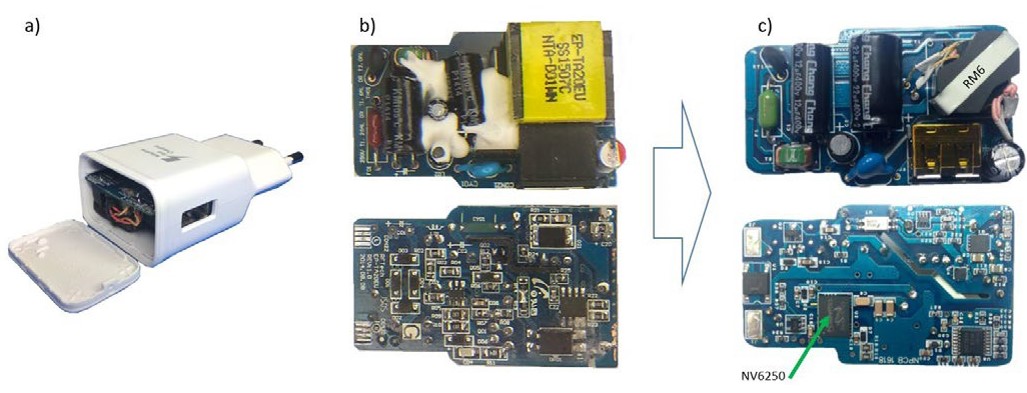
A benchmark 15 W Si-based smartphone charger is shown in Figure
3. Moving to 25 W with the same low frequency, quasi-resonant (QR) flyback topology and no increase in efficiency means a 1.4x increase in case size. Using the soft-switching ACF topology9 and with only a small increase in switching frequency to 400 kHz, yields a 25 W NV6250-based solution in the original case – a 66% increase in power density.
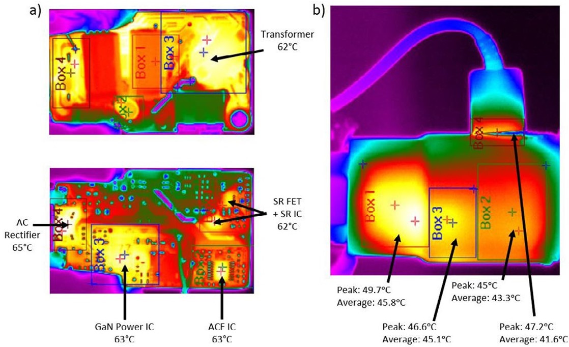
As size is reduced, efficiency must be increased to maintain a constant external case temperature. OEM specifications vary in the maximum allowable case temperature but there are cases where the limit is only 50°C (average over a 2×2 cm area). Here, to achieve the temperature rating, the system efficiency required an upgrade from ~89% to >92%.
Higher Powers, Higher Frequencies, Higher Performance
The AllGaN platform offers great flexibility for additional features / functions and also in alternative die sizes to optimize RDS(ON) for specific application power levels. MHz-switching topologies have been implemented from 25 W to 3 kW using DSP controllers. New, faster ASICs will come to market during 2017 to increase switching frequencies beyond the example 400 kHz – and so further reduce sizes – for high volume, cost-sensitive, consumer applications. By integrating the critical level-shifting, bootstrap and dual drive functions, all in GaN, the half-bridge challenge has been met and the path to MHz high- voltage power systems has been cleared.
This technical article appears on https://www.bodospower.com/
(Endnotes)
1 “Efficiency standards for external power supplies”, CUI, http://www.cui.com/efficiency-standards
2 USB-PD v3.0 Table 10-7, within USB v3.1 zip file http://www.usb.org/developers/docs/
3 TDK/EPCOS N59 : https://en.tdk.eu/tdk-en/374108/tech-library/ar- ticles/products—technologies/products—technologies/low-losses- at-high-frequencies/1206400
4 Hitachi Metals ML91S :
http://www.hitachi-metals.co.jp/e/press/news/2016/n0404.html
5 “Breaking Speed Limits with GaN Power ICs” , D. Kinzer, APEC 2016 keynote, https://navitassemi.com/white-papers-articles/
6 https://navitassemi.com/navitas-semiconductor-delivers- worlds-first-gan-power-ics/
7 “Next-generation GaN Isolators / Level-Shifters for High Frequen- cy, High Efficiency Power Conversion”, M. Giandalia, S. Oliver, PSMA Industry Session, APEC 2017, https://navitassemi.com/white-papers-articles/
8 Qualcomm® Quick Charge™ https://www.qualcomm.com/products/snapdragon/quick-charge
9 “Active Clamp Flyback Using GaN Power IC for Power Adapter Applications”, Xue, Zhang, Navitas, APEC 2017