SiC MOSFETs offer superior conductivity and switching performance compared to silicon due to their ‘wide bandgap characteristics and high electric-field strength. However, traditional designs using legacy planar or trench techniques must compromise between manufacturability, performance, and/or reliability. GeneSiC’s patented trench-assisted planar gate design is a no-compromise, next-generation solution; high-yield manufacturing, fast and cool operation, and extended, long-life reliability. It enables lowest RDS(ON) at high temperature and the lowest energy losses at high speeds. This enables unprecedented, industry-leading levels of performance, robustness and quality.
Designed for the system
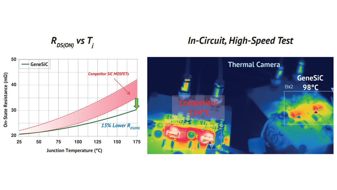
In real-life applications, the ambient temperature in a system can be up to 80C, and the power cycling of the device additionally elevates the junction temperature. This is the typical operating range of the MOSFET in real-life applications. GeneSiC MOSFETs were designed with this in mind and support the industry’s lowest RDS(ON) temperature co-efficient. In datasheets, RDS(ON) is rated at 25°C, however depending on their temperature coefficient, can significantly increase at elevate temperatures. In comparison tests, GeneSiC 1200V, 40 mΩ, in a D2PAK was compared against the comparable leading SiC MOSFET competition. The equivalent gate drive and test conditions were realized to show a true comparison. The results show that GeneSiC MOSFETs operate at 25°C cooler case temperature, which results in significantly lower losses and higher system efficiency. From a reliability standpoint, 25°C cooler operation, results in 3x longer lifetime of the device.
Recent Comments