AN011: Thermal Management of NV612x GaNFast Power ICs (gallium nitride)
![27_Pdf_File_Type_Adobe_logo_logos-512[1]](https://navitassemi.com/wp-content/uploads/2020/12/27_Pdf_File_Type_Adobe_logo_logos-5121.png)

Application Note AN011

Introduction
The latest family of Navitas GaNFast™ Power ICs include NV6123/25/27 which are available in a 6×8 mm PQFN package. This thermally enhanced package includes a large cooling pad for a low package thermal resistance and increased thermal performance. This package enables the design of high-density power supplies, especially for fully enclosed chargers and adapters with no air flow. In order to take full advantage of these thermal benefits, the PCB layout, thermal interfacing, and heatsinking, must all be designed properly.
This application note includes PCB layout guidelines and examples to help designers to design for correct thermal management for NV6123/25/27. These guidelines are intended to extract maximum efficiency and power density when using GaN Power ICs.
Overview
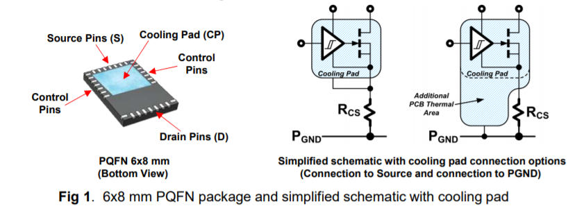
The popular NV6113/15/17 5×6 mm GaN ICs have been designed into a variety of high density power supplies. For designs with a more challenging thermal environment, this larger 6×8 mm product enables more efficient heat removal. The IC pinout of the new 6×8 mm PQFN package includes (see Figure 1) Drain pins (D), Source pins (S), control pins, and a large cooling pad (CP). The control pins manage the gate drive supply and on/off control of the GaN power FET, and most of the switching currents of the external power conversion circuit flow from the Drain pins, through the GaN power FET, and to the Source pins. A fraction of the switching current does flow through the silicon substrate of the die and out through CP. Inside the package the IC is mounted directly on the cooling pad. So the heat generated from the power losses of the GaN power FET must be taken out through the cooling pad (CP), through the solder, and to the PCB. It is helpful to use as much copper as possible to connect to the CP on the layer to which the package is soldered. Thermal vias are then used to transfer the heat to the opposite side of the PCB and/or to inner layers that have large copper planes where it can then be spread and cooled. The cooling pad is connected to the chip substrate, which can float +/-10V relative to the source. For applications where current sensing resistors are used, the cooling pad can be connected (Figure 1) to the Source pin (at the top of the current sensing resistor RCS), or can be connected to PGND to gain additional PCB thermal area for cooling.
12-19-19
Navitas Company Confidential
Page 1

Application Note AN011
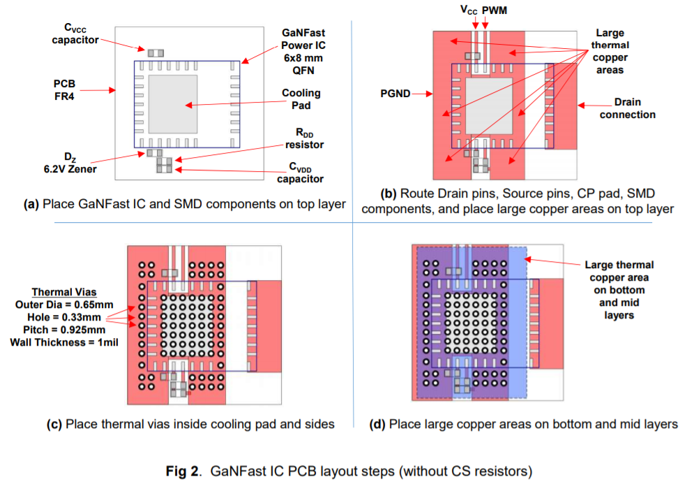
PCB Guidelines (without CS resistor)
1) Place the GaNFast IC 6×8 mm PQFN footprint on the PCB top layer.
2) Place the additional SMD components required for the control pins on the top layer (CVCC, CVDD, RDD, DZ). Place the SMD components as close as possible to the IC pins!
3) Route the connections for the SMD components, control pins, Drain pins, Source pins, and cooling pad all on the top layer.
4) Place large copper areas on the top layer at cooling pad and sides.
5) Place thermal vias inside the cooling pad and at sides.
6) Place large copper areas on all other layers (bottom, mid1, mid2, etc.).
12-19-19
Navitas Company Confidential
Page 2

Application Note AN011
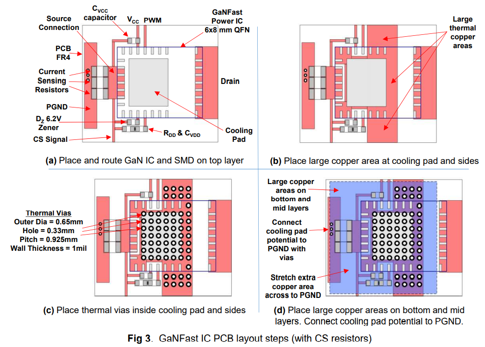
PCB Guidelines (with CS resistor)
1) Place the GaNFast IC 6×8 mm PQFN footprint on the PCB top layer.
2) Place the additional SMD components required for the control pins on the top layer (CVCC, CVDD, RDD, DZ). Place the SMD components as close as possible to the IC pins!
3) Route the connections for the SMD components, control pins, and Drain pins, and Source pins all on the top layer.
4) Place large copper areas on the top layer at cooling pad and sides.
5) Place thermal vias inside the cooling pad and at sides.
6) Place large copper areas on all other layers (bottom, mid1, mid2, etc.).
7) Connect cooling pad copper area potential to PGND with vias.
12-19-19
Navitas Company Confidential
Page 3

Application Note AN011
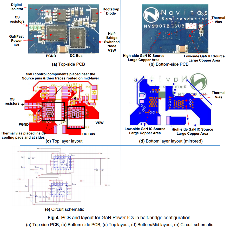
PCB Layout Example (Half-Bridge Configuration)
12-19-19
Navitas Company Confidential
Page 4

Application Note AN011
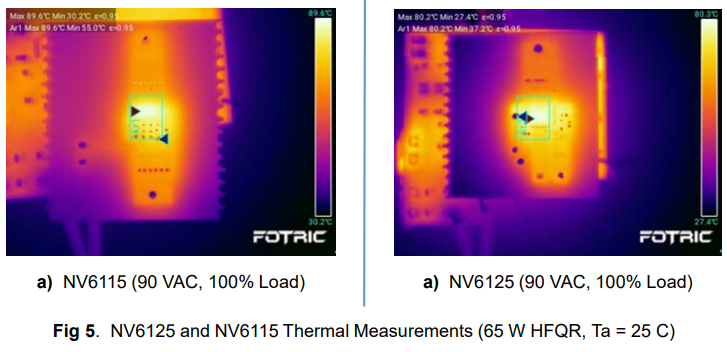
NV6125 vs NV6115 Thermal Comparison

12-19-19
Navitas Company Confidential
Page 5

Application Note AN011
45 W HFQR Planar USB-C PD Charger Example
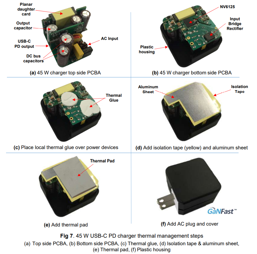
When placing the power supply PCB board into a housing, additional thermal management is required to properly conduct the heat from the PCB to the case. This is necessary to avoid high component temperatures and reduced efficiency. The following 45 W HFQR (High Frequency Quasi-Resonant Flyback) USB-C PD charger example (Figure 7) uses thermal glue placed on top of the power components, followed by isolation tape and an aluminum sheet for heat spreading. A thermal pad is then used to conduct the heat from aluminum sheet to the plastic case.
12-19-19
Navitas Company Confidential
Page 6

Application Note AN011
Product Selection Guide
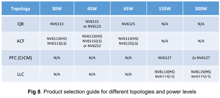
The following table (Figure 8) shows Navitas part recommendations (typical only) for different circuit topologies and power levels.
References (www.navitassemi.com)
1) Navitas GaNFastTM NV6123, NV6125, NV6127 datasheets, Navitas Semiconductor, 2019
2) Thermal Management of GaNFastTM Power ICs, AN010, Navitas Semiconductor, 2019
Additional Information
DISCLAIMER Navitas Semiconductor Inc. (Navitas) reserves the right to modify the products and/or specifications described herein at any time and at Navitas’ sole discretion. All information in this document, including descriptions of product features and performance, is subject to change without notice. Performance specifications and the operating parameters of the described products are determined in the independent state and are not guaranteed to perform the same way when installed in customer products. The information contained herein is provided without representation or warranty of any kind, whether express or implied. This document is presented only as a guide and does not convey any license under intellectual property rights of Navitas or any third parties. Navitas’ products are not intended for use in applications involving extreme environmental conditions or in life support systems. Products supplied under Navitas Terms and Conditions. Navitas Semiconductor, Navitas, GaNFast and associated logos are registered trademarks of Navitas. Copyright ©2019 Navitas Semiconductor Inc. All rights reserved
Navitas Semiconductor Inc., 2101 E El Segundo Blvd, Suite 201, El Segundo, California 90245, USA.
Contact [email protected]
12-19-19
Navitas Company Confidential
Page 7