Application Note AN020
![27_Pdf_File_Type_Adobe_logo_logos-512[1]](https://navitassemi.com/wp-content/uploads/2020/12/27_Pdf_File_Type_Adobe_logo_logos-5121.png)
Thermal Simulation Model for Selection of QFN 5×6, QFN 6×8 and QFN 8×8 Package Types
By Tom Ribarich, Sr. Director Strategic Marketing, and Bin Li, Director of Applications

Introduction
Designing a high-frequency and high-density power supply for a specific application and meeting all electrical, mechanical and thermal requirements can be a very challenging task. Part of fulfilling the thermal requirements involves ensuring that the GaN power FET junction temperature (TJ) does not exceed the recommended maximum rating during all line and load conditions, and also keeping the maximum plastic case touch temperature below its maximum allowable level. Selecting the correct QFN package type and RDS(ON)value can be a challenge in itself due to the large portfolio of products available and difficulty in predicting the final system temperatures.
This application note includes a detailed thermal setup and simulations for different power levels for QFN 5×6, QFN 6×8 and QFN 8×8 package types based on top- and bottom-cooled thermal management solutions. The results of these simulations include estimated device junction temperatures (TJ) for different device power loss (PLOSS) values. This model will help guide designers to select the correct RDS(ON) value and QFN package type for their application based on cooling method, device power loss, and resulting device junction temperature (TJ).
Overview

Figure 1: QFN 5×6, QFN 6×8, QFN 8×8 package types
PCB Layouts
2-layer PCB layouts were created for each package type under similar PCB size and copper area conditions (Figure 2). The IC components for each GaN Power IC are included in the layouts since these affect how the heat can flows away from the package in each direction. The components are placed on the top layer and connected with top layer traces (no vias). The remainder of the top side area is filled up with copper (red). The bottom layer copper fills up the complete PCB area on the bottom side. Thermal vias are then placed inside the pad area of each IC, and the heat flows from the pad down to the PCB to the top and bottom layers.
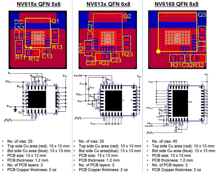
Figure 2: Schematic and PCB layouts used for thermal simulations
Thermal Model Stack-Up (Top-Cooled)
The top-cooled thermal model stack-up includes the GaN Power IC QFN mounted on the top side of a FR4 PCB (Figure 3). The heat due to the device power loss thermally conducts from the internal GaN power FET, up through the QFN plastic package, through the TIM and Mylar materials, through the copper shielding, and to the plastic case. The heat then thermally convects from the top surface of the plastic case to the surrounding ambient air. Heat also flows from the device downward to the PCB, and spreads laterally to the sides and then upward through the same materials to the plastic case. So multiple parallel paths of heat flow towards the top side are formed. The bottom area below the PCB is the inside of the power supply unit and it heats up to very high temperature that limits heat flow in the downward direction.
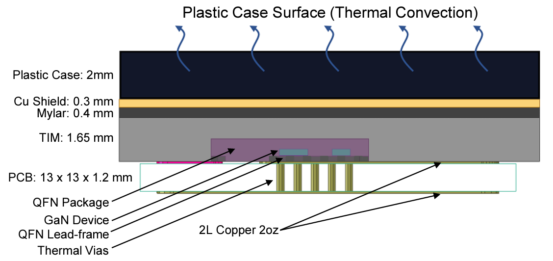
Figure 3: Thermal stack-up for top-side cooling method
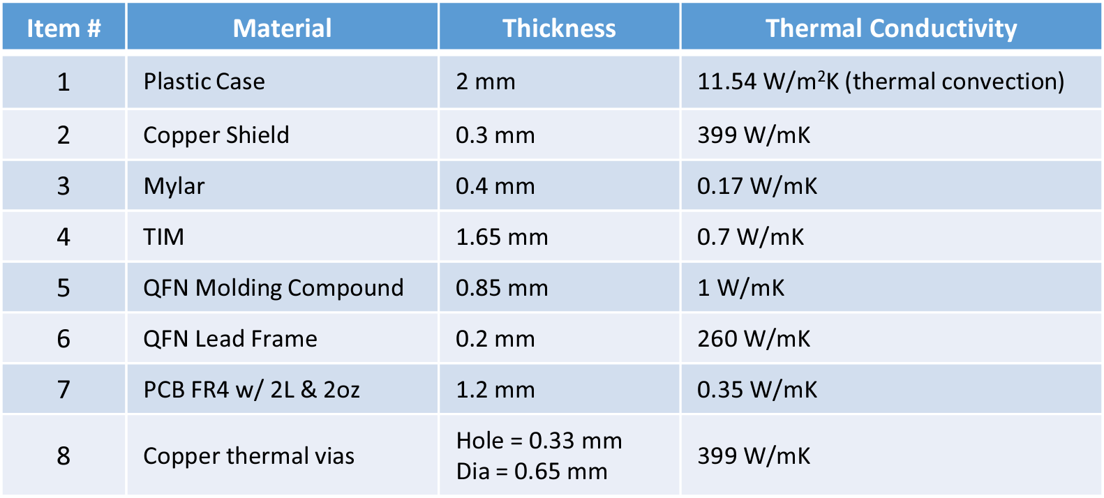
Figure 4: Thermal conductivity summary table for top side cooling materials
Thermal Simulation Setup (Top-Cooled)
The top-cooled simulation setup (Figure 4) includes the device and stack-up of materials with additional boundary conditions of 85℃ (fixed) for the other three edges of the closed power supply system. This internal ambient air will increase to high temperatures during the simulation and limit thermal conduction in the downward direction (similar to actual power supply design with power components placed on opposite side of PCB from the device). The closed power supply system is then placed into a larger closed system with the ambient air temperature set at 25℃. This setup is very similar to the thermal testing method of an actual power supply unit on the bench inside an enclosed chamber.
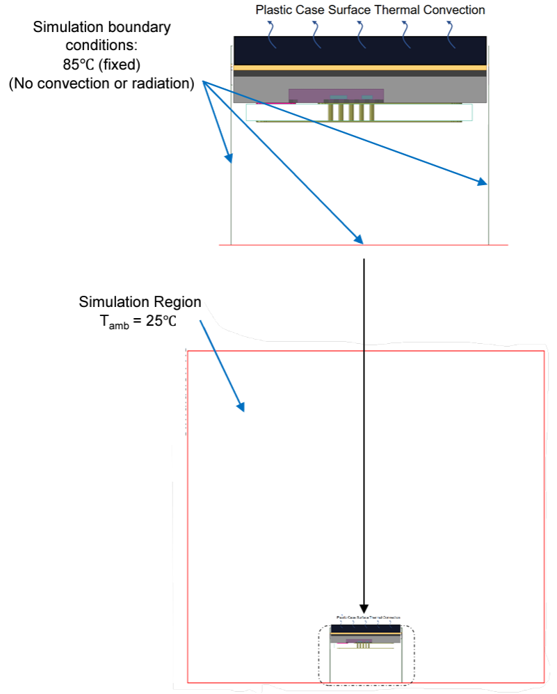
Figure 4: Thermal simulation setup diagrams for top cooling method
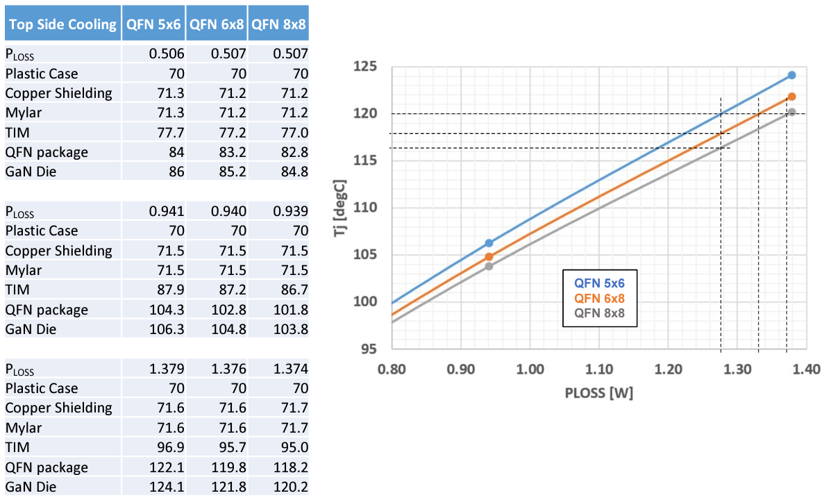
Thermal Simulation Results (Top-Cooled)
Thermal Model Stack-Up (Bottom-Cooled)
The bottom-cooled thermal model stack-up includes the GaN Power IC QFN mounted on the top side of a FR4 PCB (Figure 6). The heat due to the device power loss thermally conducts from the internal GaN power FET, down through the QFN leadframe, through the PCB and vias, through TIM and Mylar materials, through the copper shielding, and to the plastic case. The heat then thermally convects from the bottom surface of the plastic case to the surrounding ambient air. The top area above the QFN is the inside of the power supply unit and it heats up to very high temperature that limits heat flow in the upward direction.
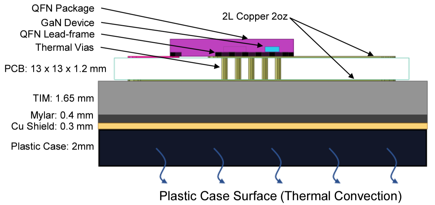
Figure 6: Thermal stack-up for bottom-side cooling method
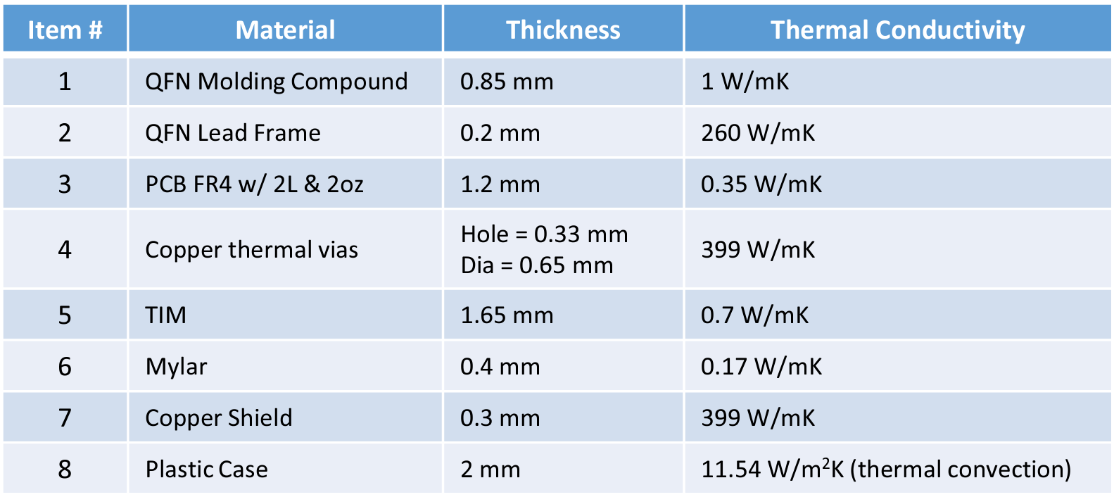
Figure 7: Thermal conductivity summary table for bottom side cooling materials
Thermal Simulation Setup (Bottom-Cooled)
The bottom-cooled simulation setup (Figure 8) includes the device and stack-up of materials with additional boundary conditions of 85℃ (fixed) for the other three edges of the closed power supply system. This internal ambient air will increase to high temperatures during the simulation and limit thermal conduction in the upward direction (similar to actual power supply design with power components placed on opposite side of PCB from the device). The closed power supply system is then placed into a larger closed system with the ambient air temperature set at 25℃. This setup is very similar to the thermal testing method of an actual power supply unit on the bench inside an enclosed chamber.
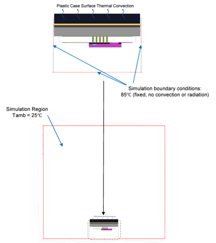
Figure 8: Thermal simulation setup diagrams for bottom cooling method
Thermal Simulation Results (Bottom-Cooled)
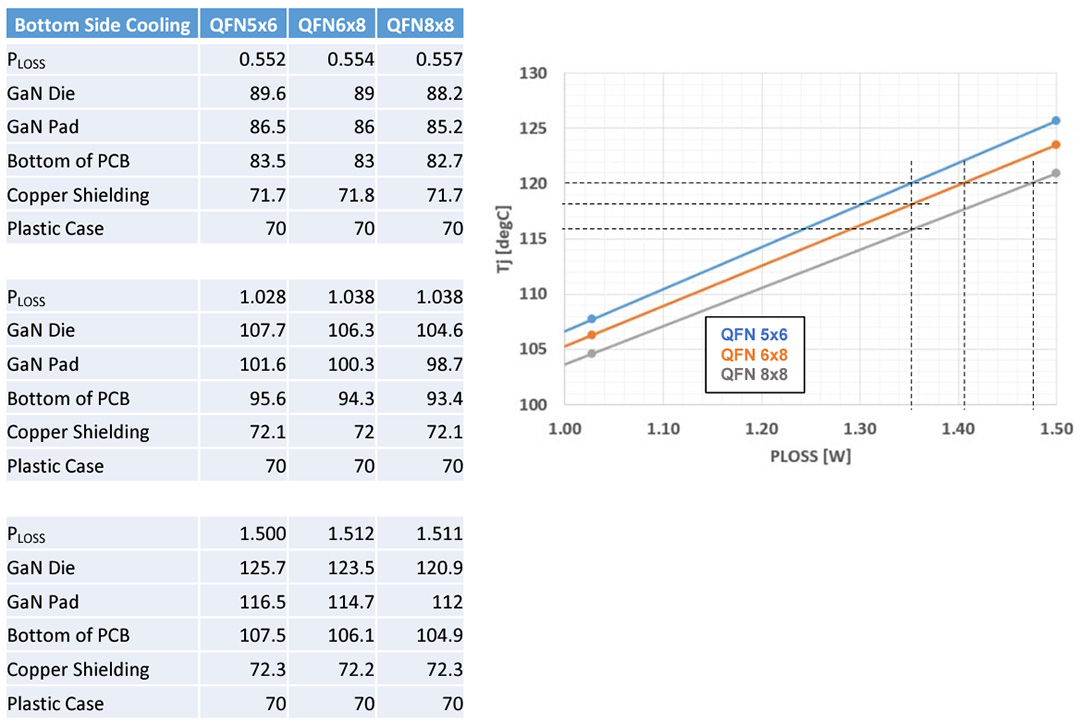
RDS(ON) and Package Type Selection
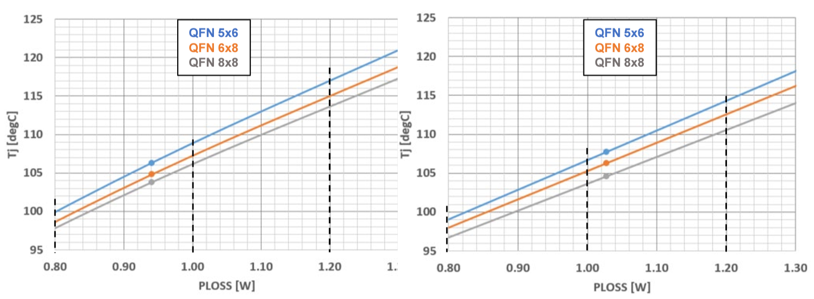
Figure 10: Top-cooling (left) and bottom-cooling (right) thermal simulation curves

Conclusions
References (www.navitassemi.com)
1) Thermal Management of GaNFast Power ICs, AN010, Navitas Semiconductor, 2019
2) Thermal Management of GaNFast NV612x Power IC, AN011, Navitas Semiconductor, 2019
3) GaNFast NV613x/NV615x, NV6169 Power ICs with GaNSense Technology datasheets, Navitas Semiconductor, 2021/2022
Additional Information
DISCLAIMER Navitas Semiconductor (Navitas) reserves the right to modify the products and/or specifications described herein at any time and at Navitas’ sole discretion. All information in this document, including descriptions of product features and performance, is subject to change without notice. Performance specifications and the operating parameters of the described products are determined in the independent state and are not guaranteed to perform the same way when installed in customer products. The information contained herein is provided without representation or warranty of any kind, whether express or implied. This document is presented only as a guide and does not convey any license under intellectual property rights of Navitas or any third parties. Navitas’ products are not intended for use in applications involving extreme environmental conditions or in life support systems. Terms and Conditions.
Navitas Semiconductor, Navitas, GaNFast, GaNSense and associated logos are registered trademarks of Navitas. Copyright ©2023 Navitas Semiconductor. All rights reserved Contact: [email protected]