Application Note AN021
![27_Pdf_File_Type_Adobe_logo_logos-512[1]](https://navitassemi.com/wp-content/uploads/2020/12/27_Pdf_File_Type_Adobe_logo_logos-5121.png)
Gate-Driver IC Selection Guidelines for GeneSiC MOSFETs
By Nabil Akel, Sr. Manager of Applications Engineering and Bin Li, Director, Application Engineering
Navitas’ GeneSiC silicon carbide (SiC) MOSFETs enable high-efficiency power delivery for a variety of applications, such as electric-vehicle fast charging, data center power supplies, renewable energy, energy storage systems, industrial and grid infrastructure. With significantly higher efficiency and faster switching than legacy silicon MOSFETs and insulated-gate bipolar transistors (IGBTs), SiC MOSFETs gate-drive requirements must be considered carefully during the design process. This application note covers the critical parameters when choosing a gate-driver IC for SiC MOSFETs.
Table of Contents
1. Gate-Drive ICs: Critical Parameters
I. Maximum gate driver supply voltage
II. UVLO Selection
III. CMTI
IV. Isolation voltage
V. Gate drive current
VI. Active Miller clamp
VII. Short-circuit protection
2. Gate Drive IC Selection
1. Gate-Drive ICs: Critical Parameters
Several important factors must be considered when selecting a gate-driver IC for SiC MOSFETs. Some examples of these are:
I. Maximum gate driver supply voltage
II. UVLO selection
III. CMTI capability
IV. Isolation voltage
V. Drive current
VI. Active miller clamp
VII. Short-circuit protection
I. Maximum gate driver supply voltage

The selected gate driver IC must support the chosen gate voltages. The requirement for the maximum supply voltage of the gate driver IC (Vcc_max), is denoted by the following calculation:

An example gate-source voltage for a G3R GeneSiC MOSFET is shown in Figure 1 below.
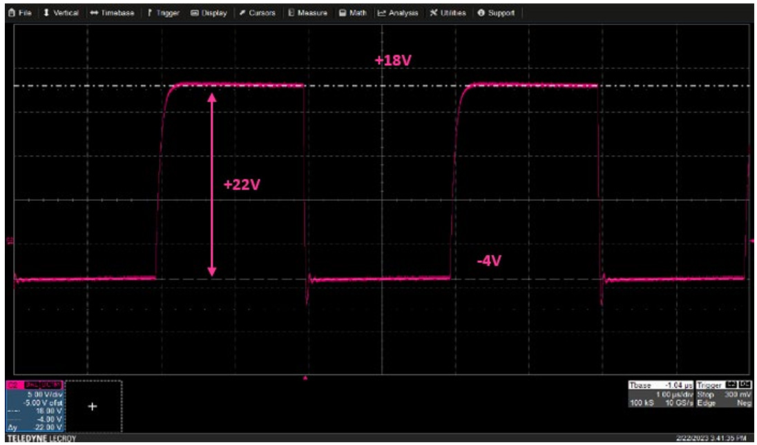
Fig. 1: Gate to source voltage waveform for 3rd generation GeneSiC MOSFET
II. UVLO selection
Figure 2 shows an example of the output characteristics of a SiC MOSFET (G3R75MT12J). It can be seen from Figure 2 that the saturation current depends on the applied gate voltage. A lower on-state gate voltage will cause the MOSFET to saturate at a lower drain current. Choosing an appropriate UVLO setting for the gate drive IC will prevent the MOSFET from entering the saturation region and thereby protecting the system.
Figure 3 shows the dependency of the on-state resistance (RDS(ON)) of the G3R75MT12J on the applied gate voltage. The typical RDS(ON) of this MOSFET is 75 mΩ at 25 °C and 15 V at the gate. If the gate voltage drops to 12 V, the RDS(ON) will increase by approximately 40%. This same trend is observed at higher junction temperatures although the RDS(ON) increase will be lower. This curve shows the importance of selecting the right gate voltage to optimize the conduction loss of the MOSFET. An appropriate UVLO setting will limit the operation of the MOSFET to the more efficient region of the curve and thereby optimizing the efficiency of the system and ensuring lower junction temperatures in the MOSFET.
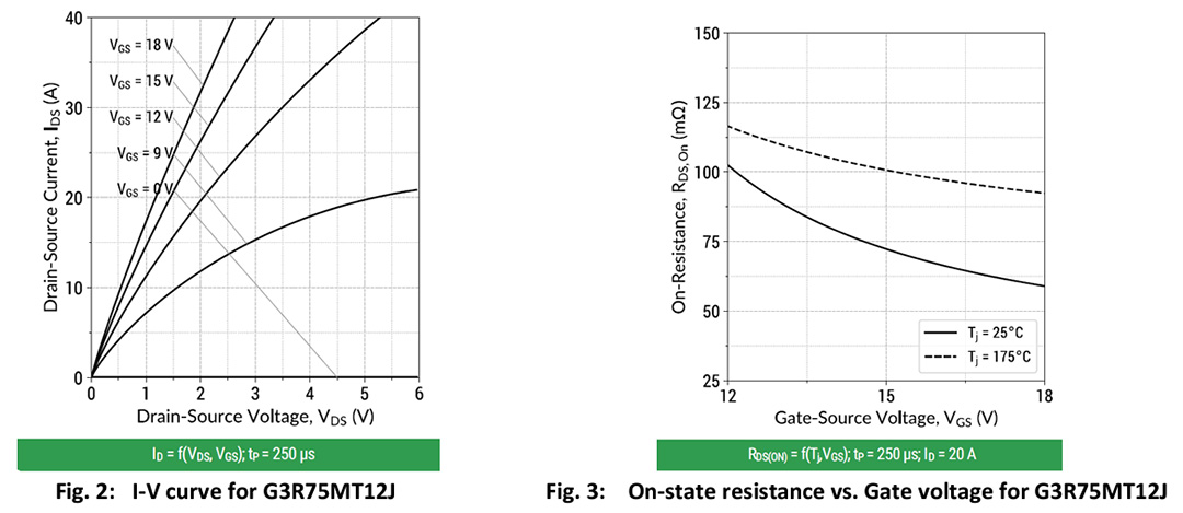
Choosing an appropriate UVLO setting is important for a safe and efficient MOSFET operation. Typically, a UVLO setting of 12 V or higher is recommended for SiC MOSFETs.
III. CMTI capability
Common-mode Transient Immunity (CMTI) is a critical parameter for selecting isolated gate drivers. CMTI is defined as the maximum allowable slew rate of the common mode voltage applied between two isolated circuits. As a rule of thumb, for an isolated gate driver, the CMTI rating should be greater than the maximum switching speed of the MOSFET in the application circuit. If this rating is exceeded, the output of the gate driver can see different fault scenarios such as a missing pulse, excessive propagation delay, false output state or latched output. Some of these failure modes can potentially be destructive. Since SiC MOSFETs can switch much faster than Si MOSFETs and IGBTs, special consideration should be taken to select an isolated gate driver with a sufficiently high CMTI rating for the target application.
Typically for high efficiency applications, fast switching speeds in excess of 50 V/ns can be reached and therefore, an isolated gate driver with a CMTI rating of 100 V/ns or higher is recommended.
IV. Isolation voltage
Different applications require different isolation voltage ratings for gate-driver ICs. This rating depends on the working voltage, and isolation requirement (functional/basic/reinforced) amongst other factors.
Typically, several isolation voltage levels are available, from 1 kVRMS to 5.7 kVRMS. The designer should select an isolator or isolated gate driver with the appropriate ratings to meet their isolation needs according to their application.
V. Gate drive current
Source and sink currents are the maximum currents that the gate driver can supply during turn-on and turn-off respectively. To switch the MOSFET with desired switching speed, it is important to select a gate driver with the correct drive current capability. A typical driving circuit is shown in Figure 4.
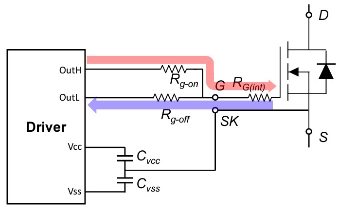
Fig. 4: Typical driving circuit of a SiC device
The required 𝐼g_on (source current) and 𝐼g_off (sink current) during turn-on and turn-off can be calculated by the equation shown below.
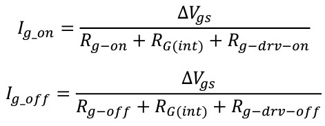

RG(int) is the internal gate resistor of SiC MOSFET, which can be found in the datasheet. For example, the RG(int) of G3R40MT12J is 1.2 Ω as shown in Table 3 below. Smaller RG(int) values are a competitive advantage for GeneSiC MOSFETs compared to other devices in the market.

Using G3R40MT12J as an example, the recommended turn-on and turn-off gate-to-source voltages are +18 V and -3 V. With 6.8 Ω Rg-on and 3.3 Ω Rg-off as the external gate resistors, the required source and sink gate currents, respectively, can be calculated as shown below:
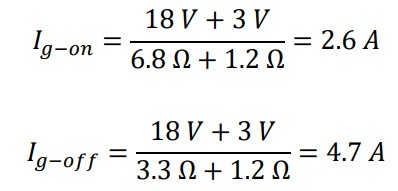
To make sure that turn-on and turn-off speeds can still be controlled by the external resistors, the source and sink current capabilities of the gate driver in this case should be greater than 2.6 A and 4.7 A respectively. Otherwise, the gate driver IC becomes the limiting factor for the switching speed.
An example of how the gate driver IC’s driving capability impacts the switching speed is shown below. Here, the device under test is the G3R40MT12J. The driving capabilities of the two gate drivers (Si8275 and SLMi8233) used for this test are shown in Table 4.

However, when we increase the external gate resistance, the difference becomes smaller since the gate driver’s capability is no longer the limitation, as shown in Figure 6.
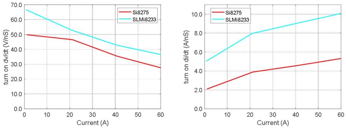
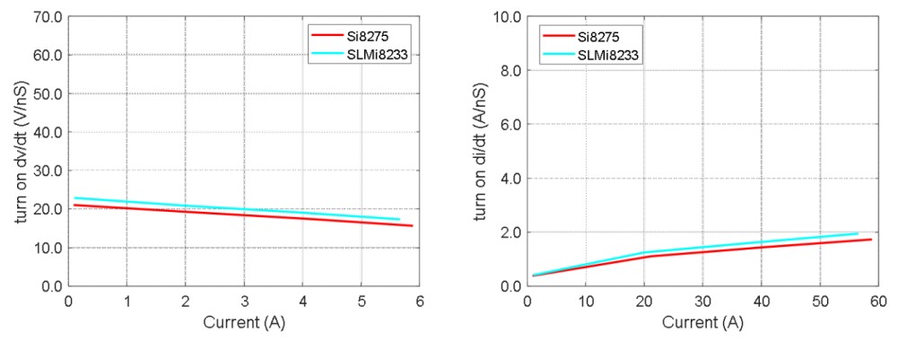
Fig. 6: Turn-on comparison between Si8275 and SLMi8243 @20𝛀 Rg-off
VI. Active Miller clamp
In bridge topologies, high switching speeds can cause voltage spikes to appear on the gate due to the induced current flowing through the Miller capacitor of the MOSFET. This effect is demonstrated in a boost converter in Figure 7 below.
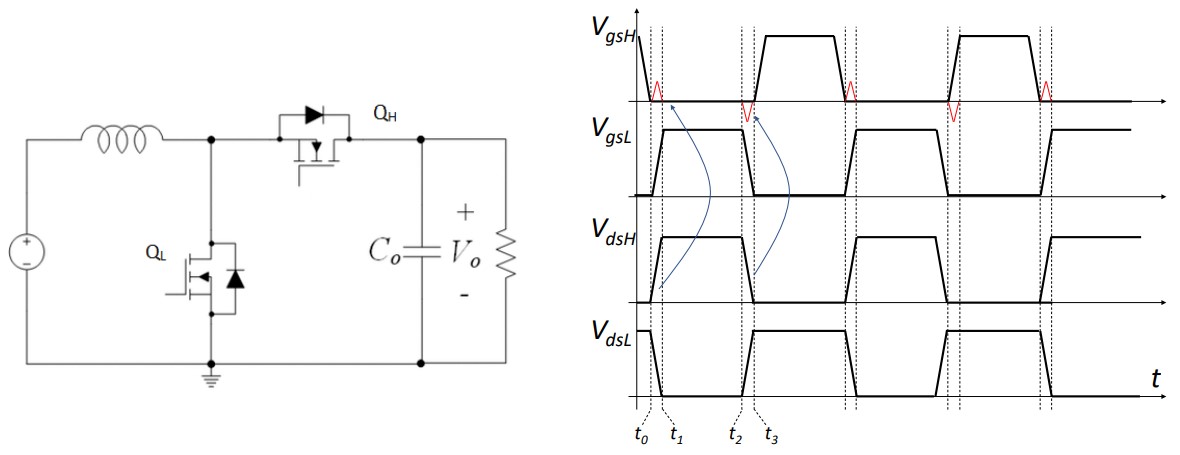
Fig. 7: Miller capacitor induced gate-to-source voltage bounce.
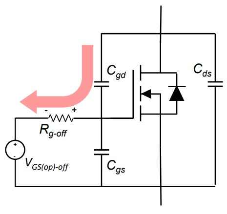
Fig. 8: Miller capacitor induced gate-to-source voltage bounce
The peak of the induced voltage bounce can be calculated by,

It can also be seen from the above equation that a negative off-state gate voltage (VGS(op)-off) can mitigate the parasitic turn-on issue by increasing the safety margin from the off-state voltage of the gate to the threshold voltage.
Another way that this issue can be mitigated is by using an active Miller clamp (Figure 9).
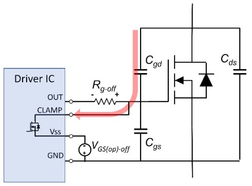
Fig. 9: Gate driver with miller clamp circuit
VII. Short-circuit protection
SiC MOSFETs have stringent short circuit protection requirements as compared to Si MOSFETs and IGBTs. As a result, for some applications, a fast and reliable short circuit protection circuit is needed to ensure a robust system operation.
The most-commonly used short-circuit protection method, which is available in many gate drivers, is desaturation detection (DESAT). The DESAT circuit senses the on-state drain-source voltage and uses this to prevent the device from entering the deep saturation region.
The response time of the DESAT circuit is comprised of three components:
- Blanking time or DESAT detection time
- The delay between the DESAT detection and the beginning of the gate shutdown
- Shutdown time during which the gate is pulled low
Most gate drivers SiC MOSFETs can start shutting down the MOSFET 500 ns after DESAT detection. For SiC MOSFETs, it is recommended that the first two components of the DESAT response time (i.e. the time it takes from the beginning of the short circuit event until the time the gate voltage starts decreasing) take less than 1 µs.
A typical DESAT circuit is shown in Figure 10.
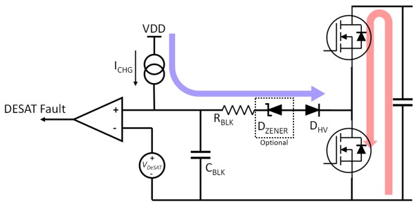
Fig. 10: Typical desaturation circuit
device.
During a short circuit event, a large current will flow through both high side and low side devices which causes a significant rise of the drain-source voltage. This charges capacitor (CBLK) to the threshold voltage (VDESAT), which triggers the comparator to shut down the device.
The drain-source voltage which triggers the desaturation protection can be calculated by,


The capacitor CBLK and can also be used to adjust the blanking time, during which the desaturation protection will not respond. The blanking time is calculated as:

2. Gate-Driver IC Selection
A non-exhaustive list of recommended isolated gate driver ICs is shown in Table 5.
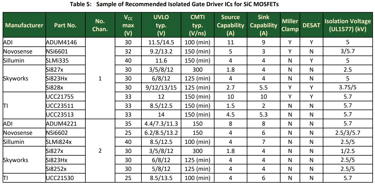
For some gate driver part numbers, there are different available suffixes to select different configurations such as UVLO levels, number of channels, isolation voltage, etc. However, the most important and relevant parameters are listed above table.
For questions regarding compatibility on gate drivers that are not listed in Table 5, you can reach out to [email protected]. For SiC device selection, electrical and mechanical models, please refer to https://genesicsemi.com/
Additional Information
DISCLAIMER Navitas Semiconductor (Navitas) reserves the right to modify the products and/or specifications described herein at any time and at Navitas’ sole discretion. All information in this document, including descriptions of product features and performance, is subject to change without notice. Performance specifications and the operating parameters of the described products are determined in the independent state and are not guaranteed to perform the same way when installed in customer products. The information contained herein is provided without representation or warranty of any kind, whether express or implied. This document is presented only as a guide and does not convey any license under intellectual property rights of Navitas or any third parties. Navitas’ products are not intended for use in applications involving extreme environmental conditions or in life support systems. Terms and Conditions.
Navitas, GaNFast, GaNSense, GeneSiC, and the Navitas logo are trademarks or registered trademarks of Navitas Semiconductor and subsidiaries. All other brands, product names, and marks are or may be trademarks or registered trademarks used to identify products or services of their respective owners.
Copyright ©2023 Navitas Semiconductor. All rights reserved.
Contact: [email protected]