GaN Drives Development of Next-Generation EVs
![27_Pdf_File_Type_Adobe_logo_logos-512[1]](https://navitassemi.com/wp-content/uploads/2020/12/27_Pdf_File_Type_Adobe_logo_logos-5121.png)
GaN Drives Development of Next-Generation EVs
By Charles Bailley, Senior Director, Global Business Development and Hao Sun, Senior Director, Navitas EV Design Center

According to a recent report1 transportation generates around 8 billion tons of greenhouse gases annually, with passenger vehicles responsible for almost half the total. As we drive towards ‘net zero’, moving to electric vehicles (EVs) is being seen as a large part of the solution. However, there remains anxiety on the part of the consumer related to range and the availability of en-route charging.
For adoption to increase, EVs must deliver safety and convenience which, in this context, relates primarily to greater efficiency to extend range, better recharging infrastructure and faster recharging times. The levels required are unlikely to be met with silicon devices, so engineers are turning to wide bandgap (WBG) materials – especially gallium nitride (GaN).

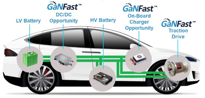
Figure 1: Applications for GaN power semiconductors in EVs
GaN can increase charging speeds threefold when compared to silicon, making the onboard charger (OBC) a target for silicon replacement.
Typically, OBCs have power ratings between 3.7 kW and 22 kW for vehicles that use 400 V and 800 V batteries and therefore require power semiconductors rated at 650V and 1200V respectively. Using integrated GaN power ICs rather than silicon devices, designers can improve charging times and achieve higher power densities that reduce OBC size, weight and cost.
One manufacturer that Navitas works with, for example, is incorporating a 22 kW OBC featuring three times faster charging in a unit that is the same size and weight as an existing, silicon-based 6.6 kW solution.
Additionally, energy stored in the battery must be transferred to multiple subsystems including seat and window motors, wipers, audio/video, HVAC and interior lighting. This requires DC-DC converters that step down the high voltage battery voltage to 48 V or 12 V. Here, GaN will dramatically reduce losses, size and weight.
Finally, GaN also benefits efficiency, size, and weight of traction systems that convert energy into propelling the vehicle. Lower GaN switching losses eliminate costly and heavy heatsinks by reducing thermal dissipation while high switching frequencies reduce EMI filtering requirements. The result is lighter, more efficient and more cost-effective traction systems that significantly increase vehicle range.
The opportunity for GaN in EV traction is enhanced as vehicles are moving to four, independent, ‘in-wheel’ traction motors to eliminate a single motor as a point of total failure. This eliminates mechanical drive-train components, delivers four-wheel drive for traction control and safety, plus gives ‘n+3’ redundancy to carry on most journeys with minimal performance loss – or ‘limp home’. GaN’s speed delivers high efficiency, lightweight and small size for in-wheel motors, increasing overall vehicle performance and range.

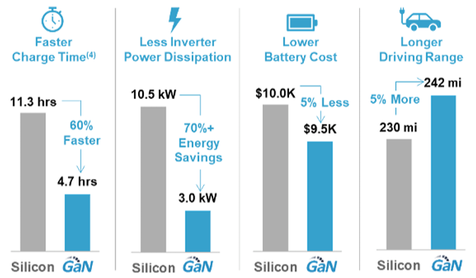
Figure 2: GaN versus silicon benefits in electric vehicles
As well as improved charging, Navitas EV customers predict the energy savings that GaN enables will translate into a range extension of at least 5%. In the EV space every additional 1% is extremely hard won, making 5% for a single technology change significant. The same estimates indicate that deploying GaN can deliver a typical cost saving on the battery of around $500 – a big step in the right direction in helping manufacturers bring the cost of EVs in line with conventional ICE vehicles.
The upshot is that by providing a solution that allows EV manufacturers to address the key challenges of charging time, energy savings, price and range then integrated GaN semiconductors will help to accelerate EV uptake. Navitas estimates that, thanks to the efficiency and cost improvements enabled by GaN, this technology will accelerate EV adoption by up to three years, which, in turn, will deliver an additional 20% reduction in road sector CO2 emissions.
GaN Choices
When considering GaN devices for EV applications, not only should the device performance be considered but also the functions (such as protection) that may be built into the device. This can reduce external circuitry and simplify design, while reducing space and cost.
‘Discrete’ GaN power transistors such as GaN E-HEMTs (enhancement mode high electron mobility transistor) are single function devices and require other circuit components to deliver a functional system. They fail to achieve mainstream adoption due to their system design complexity and poor performance in high power systems. Additionally, they lack protection features and are highly vulnerable to ESD (electro-static discharge). External circuitry can overcome these limitations but that introduces speed-limiting parasitic and lossy elements, negating the benefits of GaN.
However, integrated GaN power ICs combine several power electronics functions on to a single GaN chip and provide the most critical capabilities needed in a single device. This optimizes efficiency and power capacity, reduces complexity, lowers cost, and reduces size for system designs.
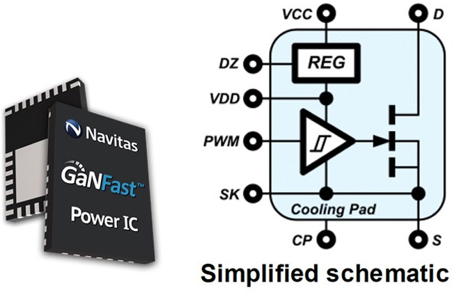
Navitas’ latest GaN power ICs, for example, monolithically integrate the GaN power FET, gate drive, and protection functions to control and protect the GaN power switch at high speeds.

Figure 3: Integrated GaNFast Power IC
These GaNFast™ devices are based on lateral 650 V eMode GaN-on-Si technology developed using the company’s proprietary AllGaN™ process design kit (PDK). GaNFast ICs are essentially easy-touse, high-speed, high-performance ‘digital-in, power-out’ building blocks that require minimal additional circuitry. As well as simplifying designs, integration enables virtually zero loss in turnoff because the gate drive loop has essentially zero impedance. At the same time, turn-on performance can be controlled and customized for the specific requirements of the target EV application.
As with most high-power conversion, designers of EV power architectures must provide effective thermal management to ensure that excess heat does not impact on performance or operating life. Highly efficient GaN-based solutions address this to some extent but, as this often leads to increased power density, the challenge remains. Thermally enhanced versions of Navitas’ GaN power ICs incorporate a large cooling pad with topside and bottom-side cooling and ensure enhanced thermal performance when using CS resistors. This also allows the use of simple and cost-effective single-layer IMS (insulated metal substrate).
Recently, Navitas announced integrated power ICs with precision sensing that will enhance efficiency, autonomy and reliability in EV power applications. Combining these with integrated drive, the proprietary GaNSense™ technology for precision and configurable sensing of system current, voltage and temperature allows GaN ICs to detect and act on high-risk conditions, protecting the IC and the system from any faults. The result is a robust, protected and reliable device that needs no external components.
Supporting the GaN Evolution
GaN technology is highly sustainable – as well as performance and efficiency improvements, GaN technology can save 80% of manufacturing and process chemicals and energy, plus more than 50% savings in packaging over conventional silicon devices. GaN can also reduce the manufacturing and shipping CO2 footprint by 90% compared to silicon, and the end application CO2 footprint by up to 30%. Each GaN power IC shipped saves net 4 kg of CO2, and GaN offers the potential to address a reduction of 2.6 Gtons CO2 annually by 2050. This equates to more than the CO2 generated by 650 coal-fired power stations, six billion barrels of oil, 560 million ICE passenger cars – or the annual electricity use of 470 million homes. In May 2022, Navitas became the world’s first semiconductor company to achieve CarbonNeutral™ company status from the leading experts on carbonneutrality and climate finance, Natural Capital Partners.
Even though it is a new technology for EVs, GaN devices have shipped in volume for years in mobile phone and laptop chargers that deliver fast charging speeds, high power densities, and small lightweight designs. Navitas, has shipped over 50 million GaN devices, with zero reported GaN-related field failures. This has resulted an unrivalled dataset that provides solid proof of quality and reliability, essential for giving EV companies confidence to embrace the technology and to create high-performance solutions for EVs in the 2kW to 20kW+ power range – solutions that deliver the same performance, quality and reliability benefits that have benefitted consumer charger applications. Additionally, Navitas announced a breakthrough 20-year limited warranty for its GaNFast technology – 10x longer than typical silicon, SiC or discrete GaN power semiconductors – and a critical accelerator for GaN’s adoption in data center, solar and EV markets. That’s why companies such as Brusa, a pioneer in electromobility, have publicly stated they will move from SiC to GaN as a key factor in reducing the size and weight of their chargers even further, while reducing their CO2 footprint.
Many expect that EVs with significant GaN content will appear in 2025 and, by then highly integrated GaN Power ICs optimized for each EV subsystem will be in use. Design of these vehicles is already well underway, requiring engineering support to use the latest GaN technology. Because of this, Navitas has opened the world’s first GaN IC Design Center dedicated to electric vehicles in Shanghai with a highly experienced team of power system designers with comprehensive capabilities across electrical, thermal and mechanical design, software development, and complete simulation and prototyping capabilities. Global EV customers are supported throughout their projects and, in partnership with OBC, DC-DC and traction system companies, the design center fully develops productizable EV power systems with the highest power density and efficiencies.
References
1) F Bill Gates (2021). How to Avoid a Climate Disaster. Penguin Random House
2) IEA (2022). Global EV Outlook 2022. https://www.iea.org/reports/global-ev-outlook-2022