GaNFast Power ICs Maximize Transient Voltage Ratings and Boost Circuit Ruggedness
![27_Pdf_File_Type_Adobe_logo_logos-512[1]](https://navitassemi.com/wp-content/uploads/2020/12/27_Pdf_File_Type_Adobe_logo_logos-5121.png)
Who Needs Avalanche?
By Tom Ribarich, Sr. Director Strategic Marketing
GaNFast Power ICs maximize transient voltage ratings and boost circuit ruggedness
Introduction
Traditional Silicon high voltage power MOSFETs have maximum voltage ratings that include maximum allowable avalanche energy levels. Avalanche breakdown limits the robustness and reliability of the power MOSFET due to the rapid and uncontrolled increase in current and the absorption of the transient or surge energy by the switch itself. GaNFast Power ICs do not have this avalanche breakdown effect so they can withstand higher transient voltage spikes and ridethrough transient conditions without absorbing any of the surge energy. This article explains the avalanche effect in silicon, how GaNFast Power ICs high blocking voltage behavior works, and compares VDSmax ratings for Silicon, GaN IC, and discrete GaN technologies for continuous and transient conditions.
Avalanche! Look Out Below!
The Avalanche effect is exactly as it sounds. Just like a small snowslide can trigger a chain reaction of collisions causing massive amounts of snow to flow rapidly down a mountain, avalanche in a MOSFET occurs when the drain voltage exceeds the maximum breakdown voltage limit (BVDSS). The high electric field accelerates carriers in the device that causes a chain reaction of collisions of carriers with atoms. This uncontrolled chain reaction causes the current flowing through the device to multiply suddenly. The resulting high current causes a rapid temperature rise within the silicon and ultimately leads to the destruction of the silicon device. This is a well-known and wellcharacterized weakness of silicon MOSFETs and has resulted in a maximum avalanche energy rating (typically in millijoules) that the device can withstand when its drain-source voltage exceeds the BVDSS limit. This rating is for a single-event only and it is encouraged by silicon MOSFET manufacturers to avoid this condition completely by using external methods such as snubbers and varistors to limit the voltage below the breakdown limit.
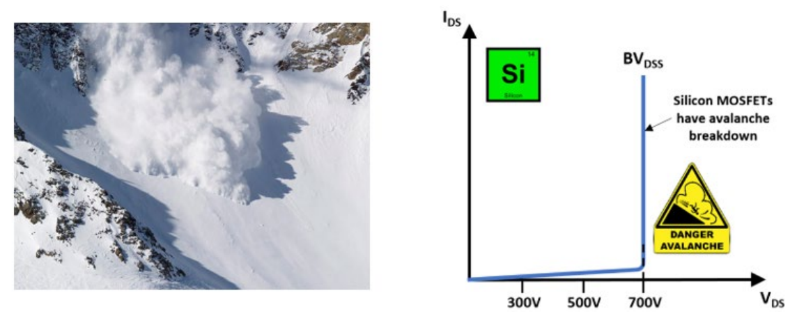
Figure 1: Silicon MOSFET avalanche breakdown effect
The silicon FET also includes a parasitic BJT that can self-turn-on during avalanche causing latchup failures. Silicon MOSFET manufacturers have gone to great lengths to characterize their devices and provide maximum avalanche ratings in an effort to work-around this inherent device weakness. But when the device is in the field, the actual surge voltage, current, time duration and no. of events (and resulting avalanche energy and device temperature) are all highly unpredictable. This places the robustness and reliability of the silicon device at high risk.
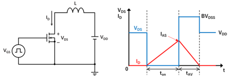
Figure 2: Silicon MOSFET avalanche unclamped inductive test circuit and waveforms
No Avalanche, No Problem!
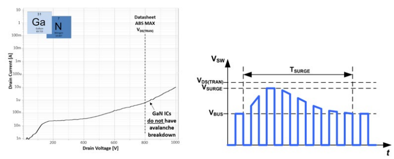
Figure 3: GaNFast Power ICs do not have avalanche breakdown and can ride through voltage surges
Over 3.5 Billion Spikes!
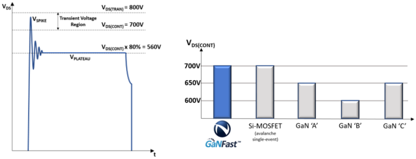
Navitas GaNFast ICs have undergone extensive robustness and reliability testing. For transient voltage spike testing, the maximum drain voltage is pulsed repetitively to a level of 800 V for a duration of 100 µsec (Figure 4). This is repeated every 2 msec for 2000 hours = 3,600,000,000 spikes! After testing, the GaN ICs are rescreened and show no change in functionality or any electrical parameters versus pre-test conditions. These results further reinforce the ruggedness of GaNFast ICs and their ability to withstand and ride through high voltage surge conditions.
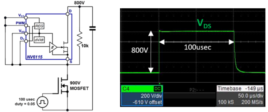
Figure 4: GaNFast Power ICs voltage spike test circuit and VDS waveform
Continuous Ratings Matter!
Silicon MOSFETs also have a 700V maximum VBDSS breakdown rating, but the VSPIKE overshoot each switching cycle can exceed this level and cause repetitive and uncontrolled avalanche. As mobile charger and adapter power levels and output voltage levels increase, these maximum voltage ratings will become even more critical and necessary in order to meet acceptable reliability standards.
Conclusion
In the past, silicon MOSFET manufacturers performed avalanche testing and provided maximum avalanche ratings due to inherent device limitations in order to enable designers to realize their products. Many applications utilized avalanche and a rugged avalanche does give a system designer some comfort about the unforeseen inductive energy spike that might occur. Avalanche can also place circuit limitations on achievable current, voltage and power levels, especially for the QR flyback topology. GaNFast ICs intrinsically block higher voltage levels and this extra voltage margin is used to ride through surges instead of avalanche. This allows circuit topologies to be extended beyond their existing range in both performance and robustness. Combining the highest continuous and transient voltage ratings together with other GaNFast IC integrated features such as gate, drive, protection, and loss-less current sensing, and an industry-first 20-year warranty, we now have a rugged, reliable and proven solution to realize high-frequency, high-density and highefficiency power supply designs. These ratings are already available today and will only continue to improve in the future.
References
1) GaNFast NV6123, NV6125, NV6127 datasheets, Navitas Semiconductor, 2019
2) GaNFast NV613x/NV615x/NV6169 Power ICs with GaNSense Technology datasheets, Navitas Semiconductor, 2021
3) IPD65R400CE datasheet, Infineon Technologies, 2016
4) Electromagnetic Compatibility, International Standard IEC 61000-4-5, Second Edition, 2011
5) Surge Energy and Overvoltage Robustness of Cascode and Direct-drive GaN HEMTs, Qihao Song, CPES, 2022