The Gallium Nitride (GaN) Revolution in Fast Charging & Power Conversion
![27_Pdf_File_Type_Adobe_logo_logos-512[1]](https://navitassemi.com/wp-content/uploads/2020/12/27_Pdf_File_Type_Adobe_logo_logos-5121.png)
The Gallium Nitride (GaN) Revolution in Fast Charging & Power Conversion
Appreciation: The Market Landscape (Si-to-GaN and Si-to-SiC)
by Stephen Oliver and Dan Kinzer
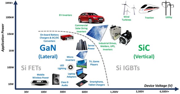
Gallium Nitride (GaN) and Silicon Carbide (SiC) are ‘wide-bandgap’ (WBG) devices. Silicon (Si) has 1.1 eV, SiC has 3.2 eV and GaN has a bandgap of 3.4 eV. As WBG material allows high electric fields, depletion regions can be very short or narrow, so device structures can have high carrier density and be packed very densely. A typical 650 V lateral GaN transistor can support over 800 V and has a drain drift region of 10-20 um, or about 40-80 V/um with a theoretical limit of 300 W/m. Silicon’s theoretical limit is 15x lower, at ~20 V/um.
SiC works well for switches above 1 kV and is optimal for higher power applications (replacing silicon IGBTs) which exploit the vertical structure for lowest resistance and which can benefit from the greatly reduced switching losses.
Lateral GaN replaces Si FETs nicely over a range of applications that require breakdown voltages from 100 V to 650 V. It offers the highest switching speed and lowest switching losses, and will enable frequencies well over 1 MHz. Fig. 1 shows how the market transition to GaN/SiC.

Fig. 1: Lateral GaN addresses traditional Si FET applications, with vertical SiC replacing Si IGBTs.
Evolution: Depletion Mode to Enhancement Mode
‘Normally-on’ depletion mode (dMode) devices require a negative gate voltage (VGS) to turn off – not a practical solution for off-line applications which would mean an immediate short-circuit across AC mains. This unwanted characteristic was mitigated by the addition of a second, low voltage ‘cascode‘ Si FET used to turn the GaN power device on and off.
However, the Si FET i ii frequency characteristics are inferior to GaN and compromise the switching performance of the combined device. Another cascode variant uses the Si FET simply as an on/off switch for the circuit, and then drives the GaN transistor directly with a negative voltage drive, leading to a complex double gate-drive solution with two supply rails. Cascoding requires at least a two chip package that presents a variety of other concerns including complex (multiple and/or stacked die) packaging, high parasitic inductance iii iv , ceramic interposers for isolation, tendency for oscillation and internal overvoltage stress due to AC and DC mismatch of the GaN & Si devices, as well as additional internal passives to mitigate these effects. This results in a reduced overall yield and ultimately a higher cost.
Enhancement mode (eMode) devices are naturally ‘normally off’ and behave in a safe, familiar way for power design engineers. A positive voltage applied to the gate will turn on the device, allowing current to flow. For eMode GaN, the voltage is around 5-6V (varies by process). If the voltage is too low the FET is not fully turned on, resulting in higher resistance and higher losses (heat). If too high, the gate structure will be damaged. With ‘discrete 3-terminal’ (gate, drain, source) GaN FETs, complex structures are typically required to control the GaN switch safely but which can be costly, consume PCB area, are a source of energy loss and also slow down the switching frequency of the application – diluting the benefits of the new WBG material.
Revolution: Low-Frequency Discrete to High-Frequency Power IC
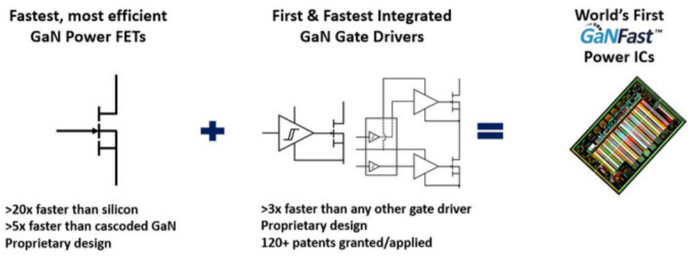
The key to improved performance (reduced loss, higher switching frequency) and rapid market adoption (simple, cost-effective designs) is to create what approaches the ‘ideal switch’, i.e. a circuit building block which translates a minimum energy digital signal into lossless power delivery. Using lateral 650 V eMode GaN, the proprietary AllGaN™ process design kit (PDK) was created which enables the monolithic integration of GaN FET, GaN analog (drive) and GaN logic into a GaN Power IC v , as shown in figure 2. This single die can then be packaged into an industry-standard, low-inductance, low cost, 5×6 or 6×8 mm QFN package for off-line AC or 400 V DC-input applications.

Fig. 2: GaN power IC integration (GaNFast).
These “GaNFast™” power ICs become easy-to-use, high-speed, high-performance ‘digital-in, power-out’ building blocks. Integration enables virtually zero loss in turn-off because the gate drive loop has essentially zero impedance vi. In addition, turn-on performance can be controlled and customized for specific application requirements. See chapter 4.10 for more on the ‘second revolution’ in power electronics.
Qualification: Proven High Reliability
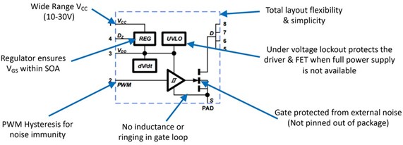
GaN-on-Si eMode discretes have been in mass production since March 2010, and have since amassed a wealth of quality and reliability data with EPC quoting 123 billion hours of operation.vii Navitas’ 650 V GaN power ICs entered the market in March 2018 with excellent device quality, reaching 5M units shipped with zero failures in June 2020vii.i Additional features and functions of the power IC increase the reliable performance of the overall application as shown in figure 3.

Fig.3: System reliability benefits from GaN power IC integration.
Continued reliability monitoring, testing and use-case-analysis reported ‘FIT rates’ (‘Failures in Time’ calculation) of only 0.54, with mean time-to-failure (MTTF) of over 233 years for a mobile fast charger application using GaN power ICs.
Transition: High-Speed Topologies
To exploit GaN Power IC capability fully, the rest of the circuit must also be able to run effectively at higher frequenciesx. Recent control ICs have increased switching frequencies from traditional 65-100 kHz up to 1 MHz+, with new controllers in development. Micro- controllers and digital signal processor (DSP) devices can also be used to implement today’s soft switching circuit topologies. A broad range of magnetic materialsxi are now available which are optimized for the 1-2 MHz range.
GaN power ICs combine frequency, density, and efficiency advantages in bridge topologies such as active clamp flyback, totem-pole PFC and LLC. With a change from hard- to soft- switching, the general loss equation for a primary FET can be minimized with GaN power ICsxii. The updated, simple equation results in improved efficiency at 10x higher frequencies.

Fig 4: Minimization of power loss in the primary power switch (FET) by moving from hard-switch to soft-switch power conversion topologies using GaN power ICs
Established topologies like the flyback converter have been updated and accelerated for high-frequency GaN. The high-frequency quasi-resonant (HFQR) flyback with GaN creates a cost-effective efficiency upgrade. The ‘active-clamp’ flyback (ACF)xiii uses an additional switch to replace the lossy ‘snubber’ circuit and delivers the highest density fast charger solution, for example Xiaomi’s 65W USB-C GaNFast charger with power density over 1.2 W/cc xiv. A further enhancement is the ‘Pulsed-ACF’ which enables the elimination of the electrolytic bulk capacitor and simple upgrade from toroidal ’wound’ transformer to low-profile ‘planar’ version which can be optimized for quiet EMI performancexv.
For systems over 75 W that require power factor correction (PFC), critical conduction mode (CrCM) boost converters are now in production for 100-300 W, with frequency ranging from 200-450 kHz – a 4x-8x improvement on silicon designs – which enables a shrink in PFC inductor and EMI. For higher powers including 1-3 kW server AC-DC, the high-frequency ‘totem-pole’ AC-rectifier-plus-PFC topology can operate at 1 MHz, with MHz LLC downstreamxvi.
Adoption: High Volume GaN
As with the transition from Si bipolar to Si FETs in the late 1970’s, the transition from Si FETs to GaN (and Si IGBTs to SiC) will not occur overnight, and while excess Si manufacturing capacity exists, the legacy technology will hang on for a few years in undemanding, low-tech applications. The adoption of GaN is most rapid in applications where size, weight and speed are critical and appreciated.
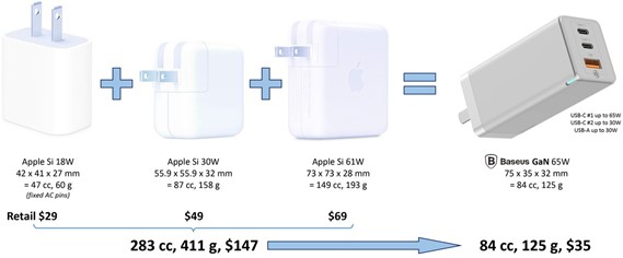
Today, the largest market for GaN is in mobile fast charging. GaN fast chargers have been released by tier-1 OEMs such as Lenovo xvii, Samsung, Xiaomi xviii and OPPO plus a broad range of aftermarket companies such as Belkin, Anker, AUKEY and Baseus. GaN power ICs enable 3x faster charging in half the size and weight of slow, silicon-based designs. For single-output chargers, GaN retail launch pricing is around half that of previous best-in-class silicon chargers xix. For the growing number of multi-output chargers – that can simultaneously charger a laptop, phone, headphones – the total price can be 3x lower, as shown in figure 5.xx

Fig. 5: GaN-based multi-output fast charger is 3x smaller, lighter and lower cost than separate, silicon-based devices (December 2019 retail pricing).
In server / telecom at higher powers (1-3 kW), 650V-rated GaN has been used in the PFC stage and primary of DC-DC stages in AC-48 V / 54 V converters. In 2017, Eltek announced the 3kW Flatpack2 SHExx,i the first in a series of GaN-based AC-48/54/60 V power supplies which achieve 98% efficiency and a 50% reduction in loss vs earlier silicon converters.
48 V distribution and down-conversion to CPU, GPU and memory for high-performance cloud services is a key area for 100V GaN. For example, for 48 V – 6 V down conversion, GaN achieves 300 W from a 27 x 18 mm open-frame DCX (LLC) at over 100 W/cc (1700 W/in3)x.xii
For additional GaN markets and applications, please see motor-control (chapter 4.6), automotive on-board fast chargers, auxiliary converters and LiDAR (chapter 4.7), and mission-critical aero/space applications (chapter 4.8).
Transformation: The Future with GaN
GaN has rapid adoption in mobile fast charger markets, with higher-power markets in development. Retail pricing for leading-edge GaN chargers is already lower than for Si, with higher performance. As design engineers become familiar with GaN and associated high- speed, high-efficiency and high-density topologies, then system innovation rates from industry will increase rapidly.
This technical article appears as a chapter in the new book: AspenCore Guide to Gallium Nitride: A New Era for Power Electronics edited by Maurizio Di Paolo Emilio, Nitin Dahad. Jan 2021.
i “Active driving of normally on, normally off cascoded configuration devices through asymmetrical CMOS“, US patent US 7,408,399 B2; Salato, Soldano,
ii “Commercialization of High 600V GaN-on-Silicon Power HEMTs and Diodes”, Parikh et al, Transphorm, IEEE EnergyTech, May 2013
iii “Evaluation of High-Voltage Cascode GaN HEMT in Different Packages“, Liu et al, VPT, 2014.
iv “Evaluation and Applications of 600 V / 650 V Enhancement-Mode GaN Devices“, Huang et al, CPES 2016.
v “GaN Matures for Industry with Monolithic Power ICs”, Power Electronics Europe, May 2016. http://www.power-mag.com/pdf/issuearchive/82.pdf
vi “Next-generation GaN Isolators / Level-Shifters for High Frequency, High Efficiency Power Conversion”, APEC 2017 Industrial Session, Oliver and Giandalia, March https://navitassemi.com/download/next-generation-gan- isolators-level-shifters%ef%bf%bdfor-high-frequency/?wpdmdl=36536&ind=1561120399092
vii “EPC eGaN FET Reliability Phase 11”, 2020 https://epc-co.com/epc/DesignSupport/eGaNFETReliability.aspx
viii “Navitas GaN IC Drives OPPO’s New Generation of Fast Charging”, July 2020 https://navitassemi.com/navitas-gan- ic-drives-oppos-new-generation-of-fast-charging/
ix “Systematic Approach to GaN Power IC Reliability”, Gandhi, APEC 2019 Industrial Session, March 2019 https://navitassemi.com/download/systematic-approach-to-gan-power-ic-reliability/ wpdmdl=36544&ind=1561100750824
x “Breaking Speed Limits with GaN Power ICs”, Kinzer, keynote APEC 2016 https://navitassemi.com/download/breaking-speed-limits-with-gan-power-ics/?wpdmdl=37075&ind=1562851197887
xi New high-frequency magnetic materials
Hitachi Metals ML91S: http://www.hitachi-metals.co.jp/e/press/pdf/2016/20160404e.pdf
ACME P61: http://www.mhw-intl.com/news/2015/03/acme-ultimate-power-materials/
xii “Welcome to the Post-Silicon World: Wide Bandgap Powers Ahead”, Kinzer, PCIM May 2016, https://navitassemi.com/download/welcome-to-the-post-silicon-world-wide-bandgap-powers- ahead/?wpdmdl=36546&ind=1561100822060
xii “Active Clamp Flyback Using GaN Power IC for Power Adapter Applications”,Xu, Zhang, APEC, March 2017 https://navitassemi.com/download/active-clamp-flyback-using-gan-power-ic-for- power-adapter-applications/?wpdmdl=37067&ind=1562850248456
xiv “Disassembly report: Xiaomi GaN Charger Type-C”, CST February 2020 (Chinese) http://www.chongdiantou.com/wp/archives/46552.html
xv “GaNFast Power ICs Enable OPPO’s 50W Mini ‘Cookie’ – the World’s Smallest, Thinnest Fast Charger”, Navitas Semiconductor, August 2020 https://navitassemi.com/ganfast-power-ics- enable-oppos-50w-mini-cookie-the-worlds-smallest-thinnest-fast-charger/
xvi “High-frequency and high-density design of all GaN power supply unit”, Yu et al, University of Texas, Austin, PCIM
xx “Here Come the GaN Chargers”, Bodo’s Power Conference, December 2019 https://navitassemi.com/download/draft-created-on-11th-february-2020-at-1142-pm/ wpdmdl=37269&ind=1581464834949
xxi “Eltek launches the Flatpack2 SHE, a Super High Efficiency power conversion module with the new CoolGaN™ technology from Infineon at its core” October 2017 https://www.eltek.com/us/insights/eltek-launches-the-flatpack2-she-a-super-high- efficiency-power-conversion-module-with-the-new-game-changing-coolgan-technology-from-infineon-at-its-core/


GaN, GaNFast and the GaNMan are all copyright Navitas Semiconductor Ltd 2021.
22 Fitzwilliam Square South, Saint Peter’s, Dublin, D02 FH68, Republic of Ireland
www.navitassemi.com
www.ganfast.com
Tel.: ThinkGaNIC +1 (844-654-2642) [email protected]