Gallium Nitride (GaN): Future Directions and Challenges
![27_Pdf_File_Type_Adobe_logo_logos-512[1]](https://navitassemi.com/wp-content/uploads/2020/12/27_Pdf_File_Type_Adobe_logo_logos-5121.png)
Gallium Nitride (GaN): Future Directions and Challenges
Device Roadmap: Integration, Integration, Integration
by Stephen Oliver and Dan Kinzer
Gallium NItride (GaN) must operate safely and efficiently in a high-frequency ecosystem to fulfil the promise of a WBG material, and higher-level device integration is a critical enabler. Integrating GaN FET, GaN analog and GaN logic creates a true GaN power IC.
GaN power IC technology was introduced by university research in the 2009 timeframe ii. Previous RF devices were developed to operate primarily below 100 V and were usually Schottky-gated depletion mode (dMode) devices though it was recognized that the gate leakage is too high for power applications. In addition, the strong industry preference is for a ‘normally-off’, or enhancement mode (eMode) device which can be used safely in off-line applications without risk of short circuit. For power applications, due to the inherent advantage of the wide bandgap technology to withstand high electric fields, most research pushed toward 600V and higher rated devices.
The ability to integrate multiple power switches on a single chip is a big advantage for GaN power ICs, e.g. in Fig. 1(a) . Since the GaN layer can be grown on different substrates, some insulating ones such as sapphire and silicon carbide were applied in early work. However, it was clear from early efforts that GaN-on-Si would enable a cost structure and an ability to use existing large diameter wafer fabs that would be a big advantage. Since silicon is a conductive substrate, this introduces the additional challenge of handling the potential of the substrate, and the way that it interacts with the power device.

Fig. 1) a: Early examples of multiple power switches on a single die, in a 3-phase circuit, b: Basic reference and comparator analog circuits.
Among the most basic analog functions developed were a simple reference and comparator ,using both eMode and dMode transistors (Fig. 1(b)), similar to the NMOS circuits common inthe 1970s. Note that no p-channel transistors are available in GaN. Another valuable featureof a power IC technology is the ability to sense temperature and react to overstresssituations.
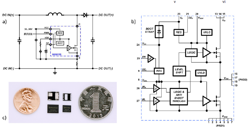
Commercially, the first full-function 650V GaN power ICs with GaN FET, GaN analog andGaN logic were introduced in 2016 and 2017 in single-switch and half-bridge formats, asshown in Fig. 2.

Fig. 2: GaNFast™ monolithic GaN power ICs, a) single-switch with driver and logic, b) half-bridge with two FETs, drive, level-shifting and boot-strap charging, and c) 6×8 mm and 5x6mm PQFN high-speed packaging.
For stable, high-efficiency, high-frequency operation it is critical to eliminate the gate-source loop impedance of the circuit. For a GaN power IC, the output of the GaN analoggate-drive is the input to the GaN FET itself, so this impedance is zero.
Half-bridge circuits are essential building blocks in the power electronics industry, used ineverything from smartphone chargers to electric vehicles. Providing power and signal to afloating high-side switch at very high frequencies can shrink magnetics and enable adramatic reduction in size, cost and weight while delivering faster charging. However, suchfrequency increases have eluded the industry as silicon devices have been too slow andsuffer from parasitic impedances between the driver and FET, high-capacitance silicon FETsand poorly performing level-shifter/isolators. Because of this, most converters still run at65-100 kHz. GaN half-bridge power ICs including critical drive, logic, protection, and powerfeatures eliminate the losses, costs and complexity associated with traditional half-bridgesolutions
At low voltages (100-300V), wafer level chip-scale packages (WLCSP) can be used as thereare no, or much-reduced ‘creepage and clearance’ requirements. This enables very small,high-efficiency, high-speed operation without the size, impedance and cost overheadsassociated with packaging. In this voltage area, GaN’s high-speed capability is an enabler invery high-frequency and sometimes mission-critical / safety-related applications such asenvelope tracking and LiDAR
As silicon developed from simple 3-terminal MOSFET to level-shifting half-bridge power ICthrough the 1980’s, GaN power ICs will continue to add features and functions in the nextfew years. Each system can be analysed to see where high-voltage GaN integration makescommercial and technical sense, for example by reducing peripheral ‘shrubbery’ componentsand/or introducing sensing and reaction within the powertrain itself. In this way, the GaNpower IC becomes an autonomous building block, reducing ‘event-to-control’ latency; e.g.safely minimizing half-bridge deadtimes, or protecting the system against over-current,over-temperature conditions.
System Roadmap: The Second Revolution in Power Electronics
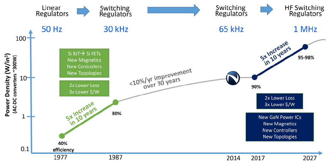
In the late 1970’s, the power electronics industry experienced an extraordinary anddisruptive change, with the introductions of new switch technology, new integratedcontrollers, improved magnetics and the industry validation of previously academic-onlypower topologies. In the following decade, the “switched-mode power supply” (SMPS)enabled a 5x increase in power density, a 5x reduction in losses in energy savings and a 3xreduction in costs (Fig. 3). The next 30 years saw incremental improvements – for example Si super-junction devices, synchronous rectification, resonant topologies – but noperformance shifts as dramatic as the first revolution.

Fig.3: Revolutions in power electronics; each triggered by the simultaneous availability/use of anew switch, integration, new magnetics and the industrialization of previously academic-onlytopologies.
As silicon developed from simple 3-terminal MOSFET to level-shifting half-bridge power ICthrough the 1980’s, GaN power ICs will continue to add features and functions in the nextfew years. Each system can be analysed to see where high-voltage GaN integration makescommercial and technical sense, for example by reducing peripheral ‘shrubbery’ componentsand/or introducing sensing and reaction within the powertrain itself. In this way, the GaNpower IC becomes an autonomous building block, reducing ‘event-to-control’ latency; e.g.safely minimizing half-bridge deadtimes, or protecting the system against over-current,over-temperature conditions. Forty years after the first revolution in power, we are witness to the second major change. The critical combination of switch (now GaN), magnetics, topology, control and integrationliberates the power designer to stretch beyond the old, slow converters to achieve onceagain the major leaps in efficiency, power density and cost.
GaN is an inherently high-speed material, and this continues as the key to power densityimprovements. While initially speed-limited by available control ICs, the introduction of newcontrollers and new topologies has seen commercial fast chargers with switchingfrequencies increasing from 50kHz (silicon) to GaN’s 400kHz in 2018 , and on to 1MHz GaNin 2020.
As noted in the white paper “The GaN Revolution in Fast Charging & Power Conversion”,soft-switching is critical to minimize or eliminate powertrain losses at high frequencies. As aresult, for 30 W – 100 W fast chargers, the venerable flyback converter upgrades to HFQR orACF, and on to ‘Pulsed-ACF’. Moving to 1 kW+ for server, the 47 kHz hard-switched boostPFC is being replaced by high-speed, soft-switching ‘totem-pole’ AC-rectifier-plus-PFCtopology that can operate at 1 MHz.
Now that a broad range of high-frequency designs are in mass production, the level oftraining and education required for design engineers to exploit GaN’s potential has fallen,and the number of designs is increasing rapidly. By the end of 2019, 50 GaN fast chargerdesigns were in production, by the end of 2020, this number could be 3x-4x higher.
Market Roadmap: Fast GaN, Fast Adoption
As with the transition from Si bipolar to Si FETs in the late 1970’s, the transition from SiFETs to GaN (and Si IGBTs to SiC) will not occur overnight, and while excess Simanufacturing capacity exists, the legacy technology will linger in undemanding, low-techapplications. The adoption of GaN is moat rapid in applications where size, weight andspeed are critical and appreciated.
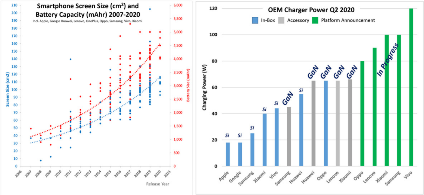
The largest market forecasted for GaN over the next 5 years is mobile fast charging, with anestimated market of $700M in 2025. While silicon designs continue to be selected for low-power, large-case, low-performance chargers from 5 W – 20 W, the majority of new higher-power, flagship smartphone charger designs (from 45 W to 100 W) are GaN.

Fig. 4: Increase in mobile phone screen size, battery capacity and associated increase in fastcharger power rating (Navitas).
Adoption has been accelerated by the increase in phone screen size cm , battery size (mAh),as shown in Fig. 4. Changes in power distribution – i.e. USB-C power delivery (PD) and programmable power supply (PPS) adoption vs. the old, low-power USB-A cables / sockets –have also been catalysts for fresh-thinking.
GaN fast chargers have been released by tier-1 OEMs such as Lenovo , Samsung, Xiaomi and OPPO plus a broad range of aftermarket companies such as Belkin, Anker, AUKEY,Hyper and Baseus. Examples of recent release are shown in Fig. 5. GaN power ICs enable 3xfaster charging in half the size and weight of slow, silicon-based designs. As of July 2020,5M GaNFast power ICs had been shipped with zero failures.

Fig. 5: Examples of fast chargers in mass production from 20 W USB-C to 100 W 2C+2A, withworld’s highest power densities (W/cc).
Business Roadmap: Positioning, Pricing and Patents
All new technologies need a beachhead application with fast time-to-market and highquantity demand to instigate supply capacity increases, new competitors, and economies ofscale to drive down costs. These lower costs then open up more price-sensitive markets.
As noted above, mobile fast chargers have achieved half the retail pricing of silicon, andwith a potential of 1.5B smartphones shipped in 2019, plus aftermarket sales, adapters forlaptops, drills, printers, drones, etc., there can be a high wafer demand to bring down costs.
Low voltage (chip-scale) GaN FET pricing reached comparable pricing with silicon FETsaround 2015
. At 650V, early (~2015) 3-terminal eMode/dMode FET pricing was around 3xthe equivalent silicon, limiting adoption to boutique applications. GaN power IC integrationand associated reduction in cost of passive components has driven system BOM costs toequal silicon today. Crude “R
DS(ON)-equivalent” GaN power IC prices are today only 1.2x Si -with high-speed performance, driver, logic and protection for ‘free’.
As new entrants appear in the GaN market, intellectual property is paramount. The pace ofinnovation is increasing with over 2,500 patents filed in 2019 across the broad RF andpower, process and device landscape. For GaN power ICs, Navitas recently announced over100 patents.
The major challenge for GaN is to break out beyond the fast charger beachhead, and useintegration, BOM-cost-equivalent pricing and performance advantages to enter laptop ‘in-box’, all-in-one PC and TV designs. Higher-power markets like server, telecom and eMobilitywill follow and continue the ‘second revolution’ in power.
This technical article appears as a chapter in the new book: AspenCore Guide to Gallium Nitride: A New Era for Power Electronics edited by Maurizio Di Paolo Emilio, Nitin Dahad. Jan 2021.
i “GaN Power IC Technology Past, Present, and Future”, Kinzer, ISPSD 2017 https://navitassemi.com/download/gan-power-ic-technology-past-present-future/?wpdmdl=37065&ind=1563179445605
ii “Integrated Voltage Reference and Comparator Circuits for GaN Smart Power Chip Technology,” K. Y. Wong et al, ISPSD’09, Barcelona, Spain, June 14-17, 2009
iii “GaN Monolithic Inverter IC Using Normally-off Gate Injection Transistors with Planar Isolation on Si Substrate,” Y. Uemoto et al, 2009 IEDM, Dec 2009
iv “GaN Single-Polarity Power Supply Bootstrapped Comparator for High Temperature Electronics,” X. Liu and K. J. Chen, IEEE Electron Device Letters, vol. 32, No. 1, pp. 27-29, Jan. 2011
v Breaking Speed Limits with GaN Power ICs”, Kinzer, APEC keynote 2016 https://navitassemi.com/download/breaking-speed-limits-with-gan-power-ics/wpdmdl=37075&ind=1562851197887
vii “Next-generation GaN Isolators / Level-Shifters for High Frequency”, Oliver and Giandalia, Industrial Session, APEC 2017 https://navitassemi.com/download/next-generation-gan-isolators-level-shifters%ef%bf%bdfor-high-frequency/?wpdmdl=36536&ind=1561120399092
viii LiDAR (Light Detection And Ranging), EPC, https://epc-co.com/epc/Applications/Lidar.aspx
ix Example IR2113 “New High Voltage Bridge Driver Simplifies PWM Inverter Design,” D. Grant, PCIM Conference 1989
x “From Science Fiction to Industry Fact: GaN Power ICs Enable the New Revolution in Power Electronics”, Oliver, Xue & Huang, Bodo’s Power December 2017 https://navitassemi.com/download/from-science-fiction-to-industry-fact-gan-power-ics-enable-the-new-revolution-in-power-electronics/?wpdmdl=37063&ind=1562849999810
xi “Navitas’ GaNFast™ Enables World’s Thinnest Travel Adapter”, Navitas March 2018, https://navitassemi.com/navitas-ganfast-enables-worlds-thinnest-travel-adapter/
xii “Silicon Chips Are History: Navitas Gallium Nitride Shrinks OPPO’s Fast Charger by 12x”, Navitas August 2020 https://navitassemi.com/silicon-chips-are-history-navitas-gallium-nitride-shrinks-oppos-fast-charger-by-12x/
xiii “SiC and GaN, two key segments for the power semiconductor industry. Quarterly Market Monitor – Q2, 2020”, Yole http://www.yole.fr/iso_upload/News/2020/PR_COMPOUND_SEMI_QUARTERLY_MARKET_MONITOR_YOLE_June2020.pdf
xiv Lenovo Legion phone launched with 90W GaNFast charger, July 2020 https://navitassemi.com/lenovo-partners-with-navitas-again-to-deliver-the-worlds-first-ganfast-90w-fast-charger-for-e-sports-mobile-phones/
xv “GaN power used in consumer electronics” TW Electronics, July 2020 https://navitassemi.com/gan-power-used-in-consumer-electronics-tw-electronics-interview-with-stephen-oliver/
xvi “Navitas GaN IC Drives OPPO’s New Generation of Fast Charging”, Navitas, July 2020
https://navitassemi.com/navitas-gan-ic-drives-oppos-new-generation-of-fast-charging/
xvii “Apple might not include a charger with the iPhone 12. Good”, The Verge, June 2020
https://www.theverge.com/2020/6/30/21307463/apple-iphone-12-power-adapter-charger-rumor-usb-c
xviii “The Future of GaN: An Interview with Alex Lidow of EPC”, Alex Lidow on EE Power, November 2019
https://eepower.com/market-insights/the-future-of-gan-an-interview-with-alex-lidow-of-epc/#
xix “GaN-on-Silicon Patent Landscape, 2020: 2,500+ Patents”, Research and Markets, January 2020.
xx “Navitas Drives the GaN Power IC Patent Landscape”, Navitas April 2020 https://navitassemi.com/navitas-drives-the-gan-power-ic-patent-landscape/


GaN, GaNFast and the GaNMan are all copyright Navitas Semiconductor Ltd 2021.
22 Fitzwilliam Square South, Saint Peter’s, Dublin, D02 FH68, Republic of Ireland
www.navitassemi.com
www.ganfast.com
Tel.: ThinkGaNIC +1 (844-654-2642) [email protected]
