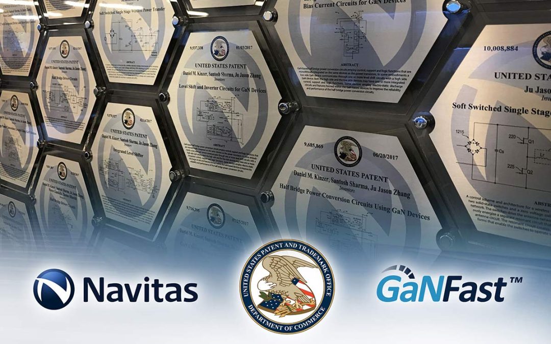
Pioneer and leader in new multi-$B semiconductor market with over 100 issued patents
EL SEGUNDO, Calif.–(PRWeb)–Navitas Semiconductor announced today that it has been issued over 100 patents in gallium nitride (GaN), a new power semiconductor material that runs up to 20x faster than old, slow silicon (Si) chips, delivering up to 3x more power conversion and half the size and weight, and creating a multi-$B market.
Navitas’ GaNFast™ Power ICs use its proprietary AllGaN™ monolithically-integrated 650V process design kit (PDK) platform to combine GaN power FETs with GaN analog drive and GaN digital logic circuits onto a single chip. As presented at the CPSS conference in 2019, The AllGaN PDK has proven to be extremely accurate comparing modelled results to actual device performance. The patents span a broad innovation range from semiconductor functional blocks (integrated gate drive, half-bridge, level-shifting, autonomous protection, etc.) and advanced low-inductance packaging, to high-frequency systems and application use cases.
“This is a tremendous milestone in the GaN power industry, and demonstrates our focus on innovation at the chip-level plus consistent drive to ensure the performance benefits can be exploited at the system-level by our customers,” said Dan Kinzer, Navitas CTO & COO, adding “Of course, a major additional factor is in the form of trade secrets and the proprietary AllGaN PDK which unlocks the high-speed capabilities of GaN and provides a robust, ‘digital-in, power-out’ system building block.”
Navitas first pioneered GaN power ICs by demonstrating monolithically-integrated single and half-bridge products at the world-leading Applied Power Electronics Conference (APEC) in 2015, going on to introduce details of the proprietary AllGaN PDK in an invited keynote at APEC 2016. A series of advanced, high-speed, high-performance reference designs and fully-qualified production release followed, leading to the world’s first commercially-released GaN-based mobile fast-charger in 2017. More than 50 GaNFast customer projects are now in mass production – including the world’s smallest 65W USB-C laptop and smartphone fast-charger by Xiaomi – and Navitas production continues to ramp steeply with excellent quality and reliability.
“Navitas began with an experienced, strong and creative technical team with an impressive record of invention and we’ve expanded that team to accelerate the growth in the patent portfolio” said Gene Sheridan, Navitas CEO, continuing “It’s a formidable IP platform and delivers leading-edge, next-generation solutions across all markets from mobile fast-chargers for laptops and smartphones to wireless power transfer, high-power IT infrastructure, autonomous vehicles, motor drives for industry, drones and robotics, plus new energy applications.”
About Navitas:
Navitas Semiconductor Inc. is the world’s first and only GaN Power IC company, founded in 2014 and based in El Segundo, CA, USA. Navitas has a strong and growing team of power semiconductor industry experts with a combined 200 years of experience in materials, devices, applications, systems and marketing, plus a proven record of innovation with over 300 patents among its founders. A proprietary process design kit monolithically integrates the highest performance GaN FETs with GaN logic and GaN analog circuits. Navitas GaNFast Power ICs enable smaller, higher energy efficient and lower cost power for mobile, consumer, enterprise and new energy markets – over 100 Navitas patents have been issued.
###
Navitas Semiconductor, GaNFast and the Navitas logo are trademarks or registered trademarks of Navitas Semiconductor, Inc. All other brands, product names and marks are or may be trademarks or registered trademarks used to identify products or services of their respective owners.
Press Contact
Navitas Semiconductor Inc.
Stephen Oliver, VP Sales & Marketing
Phone: +1 ThinkGaNIC (+1 844-654-2642)
Email: [email protected]
Recent Comments