Navitas, as a specialist in the field of gallium nitride (GaN) for power electronics, is here to break the speed limits imposed on us by legacy silicon (Si) devices.
The low switching frequencies in today’s electronics mean bulky, heavy and expensive magnetics, capacitors and energy storage elements. If those frequencies can be increased, devices can become small, light and low cost. However, today’s silicon-based electronics don’t allow for that and are stuck in the few tens of kilohertz (kHz).
Navitas wants to break through these barriers and increase speeds to a megahertz (MHz) or even ten!
Applications from mobile phone and laptops to TVs and all-in-one PCs and on up to server, telecom, new energy and eMobility can benefit with smaller size, lighter-weight, faster-charging GaN-based power.
How do we do that?
Silicon is the problem, not the answer. You’re limited to around 100 kHz and if you try to drive it harder, you get unmanageable heat, complexity and cost problems.
And then there are problems with low-frequency magnetics which just aren’t fast enough, and they get too lossy when you try to switch that fast.
Many people use hard-switching topologies which introduce a lot of switching loss, and as you go higher in frequency, efficiency drops. You can also have too much inductance in the packages and not enough thermal management.
Finally, there’s the matter of merely controlling something that’s switching that fast – old topologies and legacy control ICs can’t keep pace.
So, there are many obstacles and what are we going to do about it?
Well, the first thing to do is to solve the switch problem, and that’s what wide bandgap devices, in general, are doing, and specifically, gallium nitride (GaN).
Here’s a chart that shows you the fundamental performance of silicon (Si) devices compared to 4H silicon carbide (SiC) and GaN, i.e. critical electric field and carrier mobility.
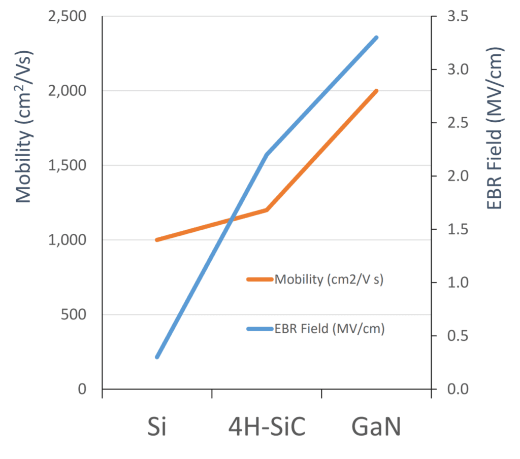
You get a two-orders-of-magnitude increase in the critical electric field, plus two times the mobility with GaN over Si.
That enables you to shrink the device dramatically, to get a very low capacitance both on the input side and on the output side. As Navitas GaN is a lateral structure where all the electrical connections to the circuit are on a single, top-side of the chip, the gate is a tiny portion of the chip area and there is very low gate overlap capacitance, making the device very easy to drive.
Given all that, we get a really low output capacitance as well. Now we have the underlying switch technology to solve this fundamental frequency problem.
But what are the other obstacles that are holding us back?
Well, some early gallium nitride devices had problems.
The earliest and easiest device to make is called a ‘depletion mode’ (dMode), normally-on device but this means an additional, Si switch is needed in series with the GaN switch – a ‘cascode’ configuration – to prevent it from automatically creating a dangerous short circuit in the system. Here, you’re actually switching the silicon device which in turn switches the GaN device, which means multiple components and insulating layers that are complex, expensive and limit the speed.
There were some early ‘enhancement mode’ (eMode) normally-off devices but due to the exposed and vulnerable ‘gate’, great care had to be taken to optimize the applied voltage: too low a voltage and the device doesn’t turn on properly – meaning a waste of GaN die area for the same resistance, or too high a voltage which meant the destruction of the discrete GaN switch and the whole system. Controlling the gate voltage meant complex, expensive drive circuits to avoid erratic, dangerous behavior and which occupied valuable real-estate, caused energy loss and slowed down the system.
What could be a better approach than what we’ve seen so far?
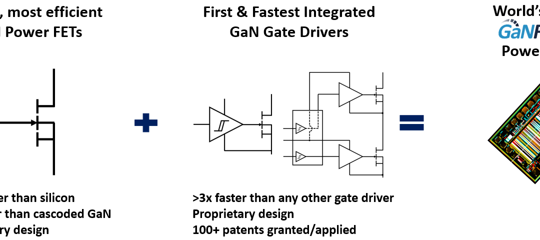
Well, what we’ve done at Navitas is to create the world’s first GaN Power IC.
We start with the world’s fastest, most efficient GaN switch – a field-effect transistor (FET) – and monolithically add analog drive and digital logic circuits integrated on exactly the same chip as the GaN power device.
Navitas’ GaN can switch up to 40 MHz, way, way beyond anything imagined for legacy Si technology. This high-sped operation means dramatic reductions in the size and cost of power conversion or fast-charging systems – at a lower system cost.
When you combine small size (high power density), high efficiency and low cost, you really have a winning solution that is changing the market and the power industry.
Here’s an example of one of our typical GaN Power ICs.
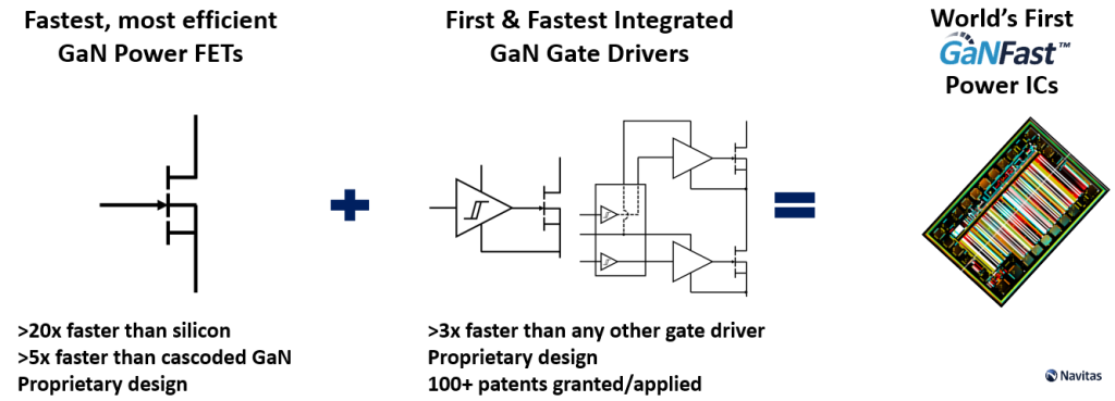
Again, this is monolithic integration, and not a multi-chip combination of a silicon driver and a gallium nitride power device.
With 20 times lower drive loss due to the inherent properties of GaN, and with a very efficient driver, we achieve an extremely-low propagation delay. Because we integrate the drive on the chip, we have zero inductance in the gate-source turn-off loop. We can control this device very well and keep it off under the highest voltage slew-rate (dV/dt) conditions up to an industry-leading 200 volts per nanosecond.
In addition to all of that, it’s so easy to use; when you want the part to turn on, simply feed in a low-power, high-speed digital ‘logic 1’ signal and it’ll turn on. With a ‘logic 0’, it’ll turn off.
It’s an easy-to-use, ‘digital-in, power-out’ building block, and as it uses a digital signal, it’s layout insensitive. All of this means easier, faster, first-time-right designs which enable faster time-to-market and time-to-profit rewards.
We also get incredibly smooth, clean, fast wave forms. Here’s an example:
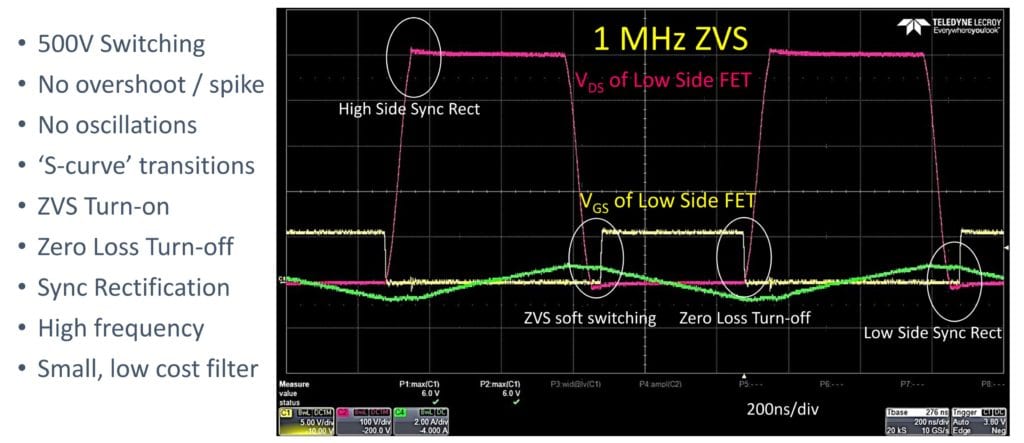
This waveform is showing a zero-voltage-switched, symmetrical ‘half-bridge’ waveform.
The pink waveform is the middle ‘switch-node’ between the two half-bridge switches, and you can see a 500-volt signal here, switching at high, MHz-frequency yet completely in control with no overshoots, no spikes, no oscillations, very clean transitions, zero-voltage-switching turn-on, and essentially zero-loss turn-off.
If you look at the yellow gate-drive form, the gate is well off before the voltage ever starts to rise on the FET, so not only do we get zero switching loss in the turn-on because of the zero-voltage-switching property of this circuit, we get zero losses in the turn-off as well.
Essentially, we’ve reduced or eliminated switching losses in this circuit so the barriers to high frequency are removed, and it’s done in a clean, cost-effective, simple way.
It’s not just about the switch, and it’s not just about the integrated drive.
The overall power system that uses this part requires more, and a critical point is that the eco-system for high-speed switching is also available today, with MHz-optimized magnetic materials and high-speed control ICs optimized for system power from 25W to kW+.
What has been done with discrete products in the past is now going to be done in a much more integrated and cost-effective way, and there are a lot of industry participants that support power electronics designers along the road to this high-frequency conversion.
We can implement lots of topologies that are soft-switching like LLC, critical-mode or boundary-conduction-mode power-factor correction, active-clamp flyback and synchronous rectification.
With additional features like dV/dt control, autonomous on-board protection, electro-static discharge (ESD) protection diodes, under-voltage lock-out and level-shifting functionality, the roadmap for monolithic integration is rich and exciting.
The barriers and speed-bumps have been removed and, with GaN power ICs, the road ahead is bright and possibly limitless. Let’s Go GaNFast!
Recent Comments