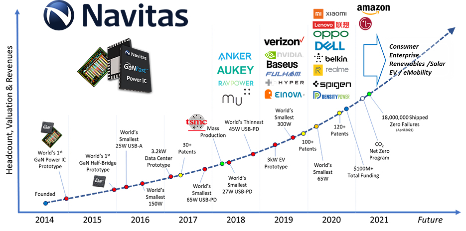
Founded in 2014, Navitas is a gallium nitride (GaN) power IC company. The Navitas goal is to ‘Electrify Our World™’ using next-generation power electronics and to enable and accelerate the transition to fast, efficient, clean forms of sustainable energy. Gene Sheridan (CEO) and Dan Kinzer (CTO) are co-founders, along with Nick Fichtenbaum (VP Engineering) and Jason Zhang (VP Applications & Technical Marketing). With major design and application centers in El Segundo, CA, Shenzhen, Hangzhou and Shanghai, and additional sales sites, Navitas has grown to over 100 employees.
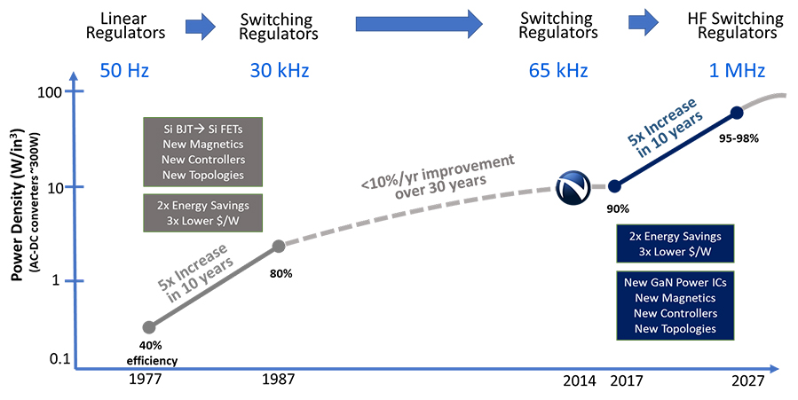
“The problem is that silicon as a power conversionplatform has hit its physical limits and it’s time for a new semiconductor – gallium nitride (GaN)– to take its place,” said Sheridan in an interview with EE Times. The integration of GaN technology will allow you to have the next smaller form factors with more power. Moreover, a worldwide Si-to-GaN technology upgrade would reduce energy loss and GaN would address a cumulative 33 Gtons of CO2 reductions by 2050.
The company is funded by the management team and top venture capitalists including Atlantic Bridge, Capricorn Investment Group and Malibu IQ. Funding to date totals over $100M. The name ‘Navitas’ derives from the Latin word for ‘energy’, which encapsulates not just the focus on developing technologies for improved and more sustainable energy use, but also the energy to accelerating a power semiconductor market that is predicted to be worth more than $13B by 2026.

Sheridan pointed out that Gallium nitride (GaN) power ICs have gone from strength to strength in what has been a turbulent 2020 for many in the power semiconductor industry. GaN has gained the market in mobile & consumer fast-charging with adoption by Lenovo, OPPO, Xiaomi, Dell and many other top-tier OEMs, plus dozens of aftermarket companies.
“With unique and proprietary integration of GaN power, GaN drive, logic and protection, GaNFast power ICs enable 3x faster charging in half the size and weight – and up to 40% energy savings vs. old, slow silicon solutions. GaNFast power ICs enable the introduction of new, soft-switching control ICs for advanced, high-frequency topologies like totem-pole and pulsed active clamp flyback,” said Sheridan.
Navitas’ GaNFast power IC technology consists of a proprietary, lateral, GaN-on-Si process design kit, with monolithic integration of GaN FET and GaN drive, plus control and protection.
650V GaNFast ICs are rated up to 800V for transients, up to 2 MHz high-speed performance and enable high power density in applications ranging from fast chargers for smartphones, laptops and tablets to TVs, data centers, electric vehicles, eMobility and renewable energy.
Sheridan highlighted that Navitas is committed to sustainability through the Navitas NetZero program. Gallium nitride delivers CO2 savings from the very start of GaN power IC manufacturing – with a 10x smaller CO2 footprint than equivalent silicon devices. “Navitas is working across a broad range of customer partnerships to assess and reduce total lifecycle footprint. By 2050, GaN is expected to address a 2.6 Gton per year reduction in CO2,” said Sheridan.
The Navitas management team has a track record of innovation (300+ patents) and business creation (>$4B) in power electronics. Top-tier customers include Dell, Lenovo, Xiaomi, OPPO, LG and many more. By April 2021, Navitas had shipped over 18,000,000 GaN power ICs, with zero (0) failures.
“Reliability is critical in all markets, and especially so in data center, EV and solar. Customers not only demand clean lifetest results at initial production release, but hard data on units shipped, field performance and ongoing reliability monitoring to prove long lifetime in harsh, performance-critical environments,” said Sheridan. “Our proven strength in mobile and consumer can be leveraged into higher-power markets.”
With over 75 customer projects in mass production, and over 150 more in development, the current focus of Navitas as Sheridan told us, is on accelerating the steep production ramp while maintaining excellent quality and on-time delivery metrics. Parallel challenges include increasing the rate of technological innovation (patents) plus launching next-generation devices with higher efficiency and additional GaN power IC functionality. The new product lines will enable advanced high-speed topologies that will continue the roadmap of efficiency, power density and reduced system costs – enabling expansion into new, higher-power markets such as EV, solar and 5G communications. “While discrete GaN FETs are susceptible to destruction or degraded lifetime from excess voltages, GaN power ICs have integrated protection circuits that set the benchmark for reliability and performance over the life of the targeted end equipment. GaN’s future continues along the path of integration, with more features, more functionality, more value to the power electronics designer – and ultimately for all of us – as we accelerate away from fossil fuels and “Electrify Our World.”

Recent Comments