[A translation from the original article in Chinese, associated with the live-stream training webinar by Navitas Semiconductor’s Yingchun (Michael) XU, 5-19-20.]
Jiwei Live Broadcasting Room has received a lot of attention and praise from the industry since its opening.
Jiwei hopes to turn the “Jiwei Open Course” into the most professional and high-quality online training course in China’s ICT industry, deepen the integration of industry and education, and help the development of China’s ICT industry.
On May 19 (Tuesday) at 10:00 am, the thirteenth “Jiwei Open Class” was held by Yingchun (Michael) XU, Senior Director of the Navitas Semiconductor Application Center in Hangzhou, China.
Click here to watch the playback
In the past thirty years, electronic power equipment has been designed with traditional silicon devices, with low switching frequency and high power consumption, and requires a large number of hand-made passive components. The problem with this traditional design is that the system is bulky, inefficient, and high cost. According to statistics, the annual energy consumption of traditional electronic equipment accounts for nearly 20% of the world’s total power generation.
In the process of power conversion, higher switching frequency can achieve smaller size and lower cost. Therefore, gallium nitride (GaN) devices with faster switching speed and higher efficiency may completely replace traditional silicon devices.
Navitas Semiconductor [known as ‘NanoMicro’ in Chinese] is the world’s first and only GaN Power IC manufacturer. Here, Navitas explain the technical value of GaN, popular applications, and the improvement of switch performance from the perspective of “Navitas Gallium Nitride Power Chip Integration and Applications”. The number of people who watched this open class online in the Aiji Micro APP exceeded 10,000!
Technical background of GaN
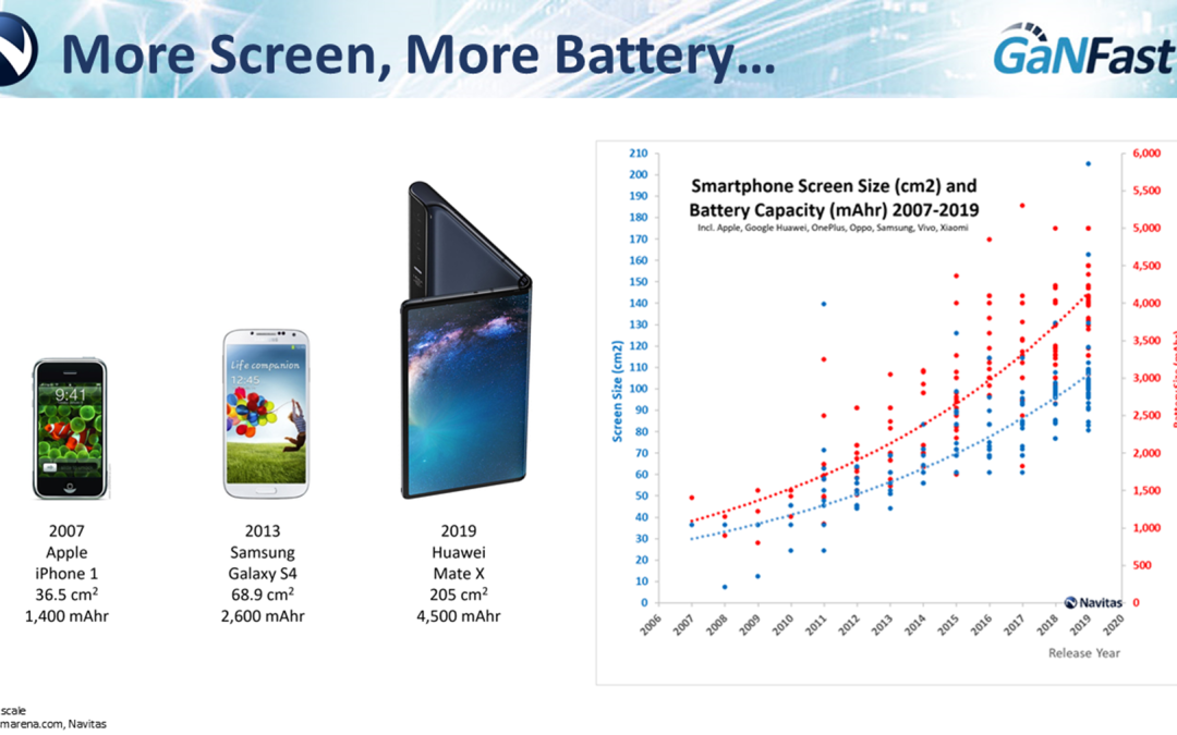
As smartphones have advanced and provided more features, with the improvement of mobile phone screens, processors, networks, wireless connections and data access energy consumption has increased.
In the process of continuously upgrading fast-charging technology, from the perspective of its basic materials, the charging efficiency of traditional silicon (Si) devices and gallium nitride devices has diverged. Compared to legacy Si, the technical value of GaN is that it can achieve a higher switching frequency, thereby reducing the volume of many passive devices, achieving higher power density and high efficiency.
In the commercial field, a 65W GaN charger released by Xiaomi for the Mi 10 and Mi 10 Pro using Navitas GaNFast power ICs not only has high charging efficiency, small size and portability for smartphone users can also charge laptops. In addition, in the past year, Baseus and Navitas launched several medium- and high-power charger products, all of which have been mass-produced, and mass production means the design specifications of the entire product reliability, EMI and manufacturability have also been fully verified.
The advantages of GaN
According to XU Yingchun, the main advantages of GaN include low RDS(ON) for the same chip size; no reverse-recovery loss; low gate-drive charge Qg, low drive loss, small parasitic junction capacitance COSS, capacitive loss Low; fast switching speed and other characteristics.
It is worth noting that when the GaN device is turned off, it can also be reverse-conducted. For 650V Navitas GaN, the typical value of VSD is only 3.5V, with zero Qrr loss in reverse conduction.
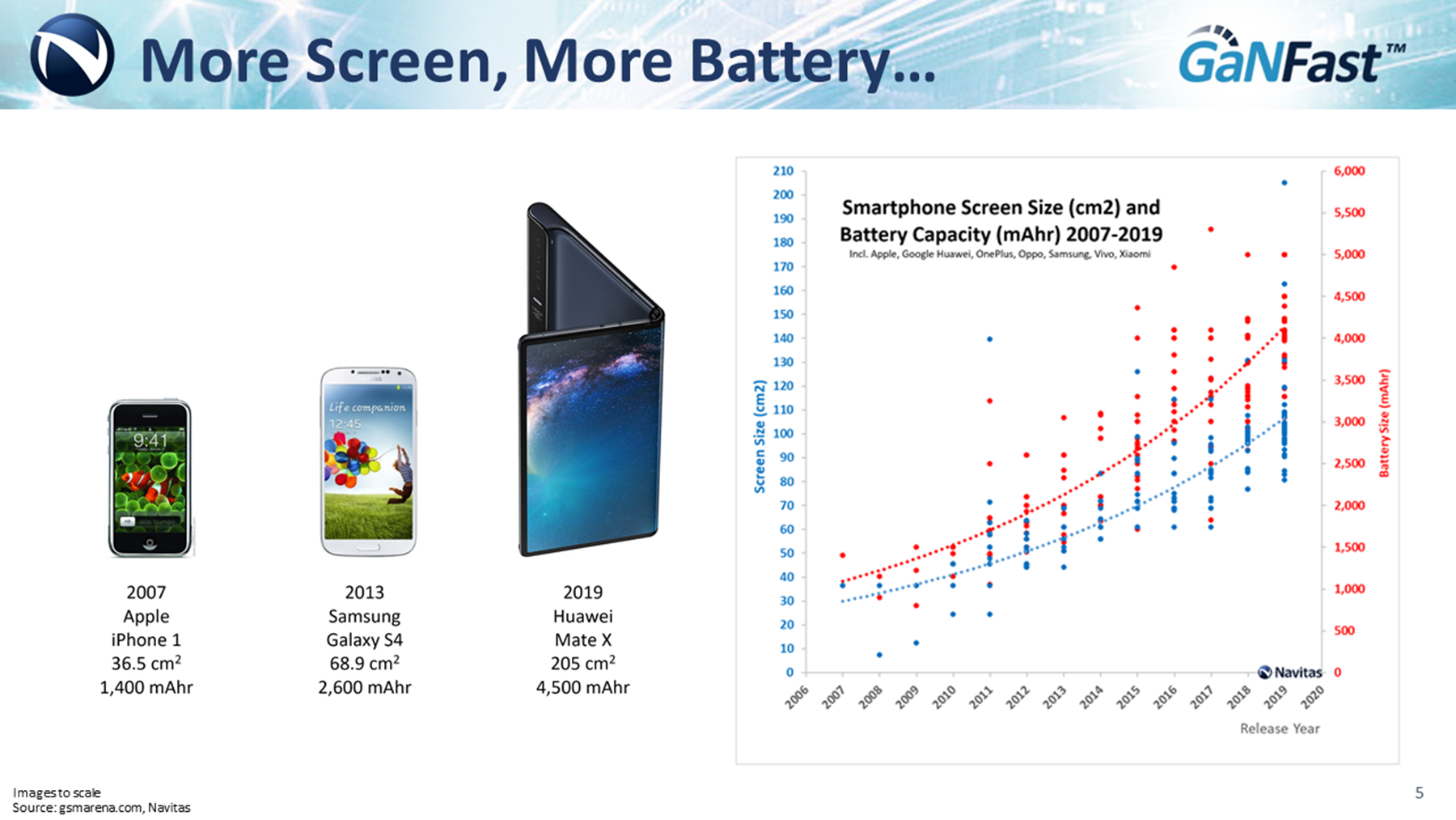
Introduction of GaN Integrated ICs
Talking about the technology of power gallium nitride (GaN), the first thing to understand is the characteristics of the physical material of gallium nitride. Its high voltage, high frequency, temperature resistance and other aspects are far superior to the characteristics of silicon. GaN devices, can be divided into two types on the market, the modern mainstream version uses enhancement-mode (eMode) FET switches, with some legacy depletion-mode (dMode) products available.
The advantages and disadvantages of the two types of GaN devices – eMode and dMode – are mainly compared from multiple angles such as switching frequency, die packaging and dV/dt control.
Xu Yingchun said that Navitas launched the first power chip in the world, which includes the analog gate driver and digital logic circuits, and combined with the gallium nitride power switch (FET), which can provide up to 40 MHz switching frequency and achieve more than 5 times the power density, compared with silicon-driven systems. Due to its simple structure, system cost can be reduced by 20%.
At the same time, Xu Yingchun emphasized that Navitas GaN power ICs have been in mass production since the first quarter of 2018, and that client products have been in mass production for over two years.
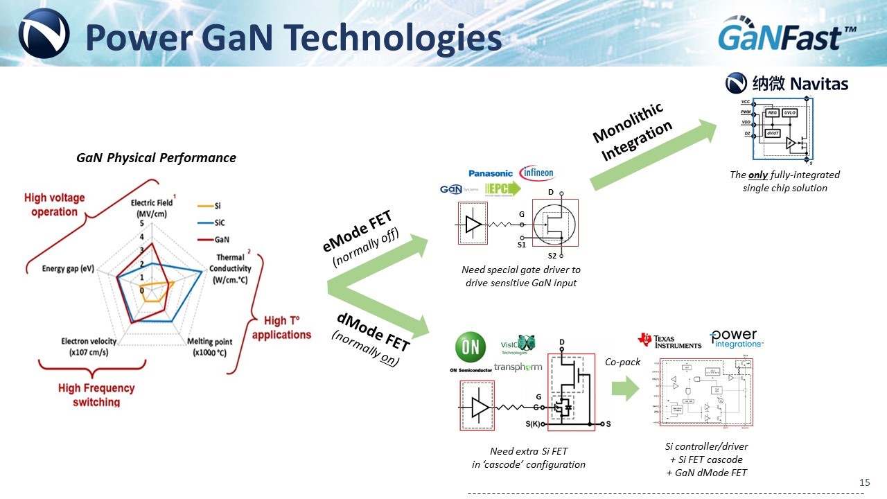
In addition, the integrated driving features of Navitas GaN power ICs are shown in the following:
Not only that, in addition to single-chip GaN power ICs, Navitas also launched a series of half-bridge GaN power IC products, with two GaN power FETs, two GaN drivers, signal and power supply bootstrap lines, etc. Half-bridge GaN power ICs can achieve stable, no-overshoot outputs.
GaN improves the performance of switching power supply
The most important way GaN can improve the performance of switching power supplies is that it can significantly reduce the losses in the switching process.
Xu Yingchun introduced that GaN has 85% lower turn-on loss and 95% lower turn-off loss than Si. This means that as the switching frequency increases, the actual switching losses are greatly reduced. However, if the switching frequency is very high, the turn-on loss cannot be ignored, and a soft switch needs to be added.
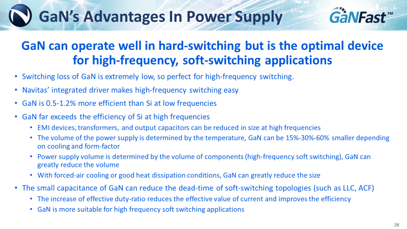
Reviewing GaN and Si versus frequency, it is clear that GAN is the optimal solution for high-frequency, soft-switching applications.
High-frequency GaN design notes
Regarding the design challenges of GaN high-frequency switching power supply, it mainly focuses on two parts: transformer and EMI.
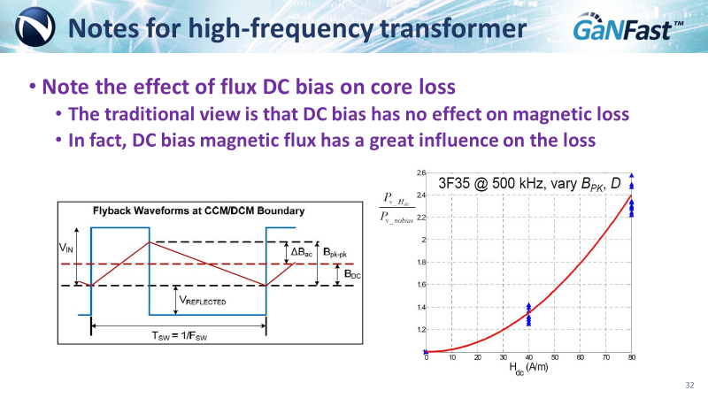
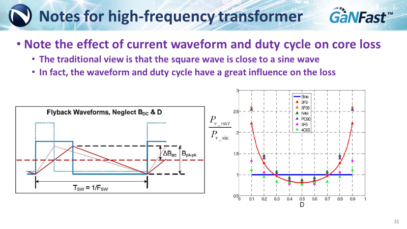
For high-frequency transformers, first look at wire selection. Based on severe adhesion and proximity effects, it is best to use 0.05-0.08mm Litz (stranded) wire for coils above 200k. Secondly, for core loss, main influencing factors include current waveform, duty cycle, magnetic flux and DC bias.
In the current market, various magnetic companies have launched high-frequency cores. “We hope to build a better eco-system, where the Litz wire or the magnetic core, can be a shared resource of suppliers.” Xu Yingchun said.
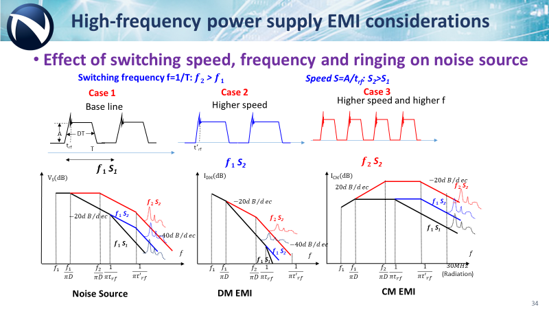
Finally, we will discuss the relevant advice for high-frequency GaN power supply EMI, mainly the impact of switching frequency and ringing on noise sources. In addition, high dV/dt and di/dt make spatial coupling heavier, so that the design requirements of the switching power supply are higher.
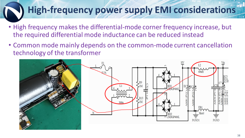
To solve these issues, EMI countermeasures proposed by Navitas are that differential-mode corner frequency increases at high frequency but the required differential-mode inductance can be reduced; while common mode mainly depends on the transformer common-mode current-cancellation technology.
For example, from the primary side switching waveform VDS noise source, we can see that the common-mode current is coupled from the primary side to the secondary side through the primary and secondary parasitic capacitance. There are more issues to note, among them that the common-mode current-cancellation uses the principles of shielding and balancing, combined with auxiliary windings, shielding layers, etc. The number of turns and line width depend on the system parameters such as the distribution of transient voltage and the thickness of the insulating layer, which can be fine-tuned to reach the optimal value.
[For additional information on designing with Navitas GaNFast power ICs, please refer to application notes, technical articles and device datasheets on www.navitassemi.com.)
Recent Comments