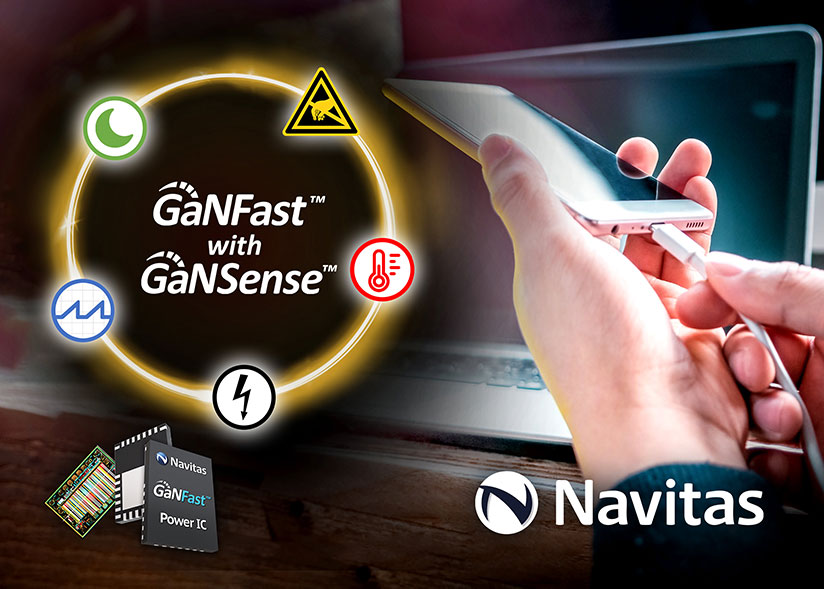
GaNSense delivers highest efficiency and reliability through real-time autonomous sensing and protection for the $4B mobile charger and consumer market
El Segundo, CA – November 5th, 2021— Navitas Semiconductor (Nasdaq:NVTS), the industry-leader in gallium nitride (GaN) power integrated circuits (“ICs”) has announced the launch of GaNFast™ power ICs with GaNSense technology. GaNSense technology integrates critical, real-time, autonomous sensing and protection circuits which further improves Navitas’ industry-leading reliability and robustness, while increasing the energy savings and fast-charging benefits of Navitas’ GaN IC technology.
Gallium nitride (GaN) is a next-generation semiconductor technology that runs up to 20x faster than legacy silicon and enables up to 3x more power and 3x faster charging in half the size and weight. Navitas’ GaNFast™ power ICs integrate GaN power and drive plus protection and control to deliver simple, small, fast and efficient performance.
GaNSense technology integrates real-time, accurate and fast sensing of system parameters including current and temperature. This technology enables a patent-pending loss-less current-sensing capability, which improves energy savings by up to an additional 10% compared to prior generations, as well as further reducing external component count and shrinking system footprints. In addition, if the GaN IC identifies a potentially dangerous system condition, the IC is designed to transition rapidly to a cycle-by-cycle sleep-state, protecting both the device and the surrounding system. GaNSense also integrates an autonomous standby-power feature which automatically reduces standby power consumption when the GaN IC is in idle-mode, helping to further reduce power consumptions, which is especially important to the growing list of customers aggressively pursuing their own environmental initiatives.
With the industry’s tightest current-measurement accuracy and GaNFast response time, GaNSense technology means reducing dangerous over-current spikes by 50% and reducing time in the ‘danger zone’ by 50% compared to previous best-in-class solutions. GaNFast monolithic integration delivers dependable, glitch-free operation with no ‘ringing’, for improved system reliability.
“From detection to protection in only 30 ns, GaNSense technology is 600% faster than discrete GaN implementations,” said Dan Kinzer, COO / CTO and co-founder of Navitas. “This next generation from Navitas provides a highly-accurate and effective defense against potential system failure modes. Couple that with immunity to transient voltages up to 800V and tight gate waveform control and voltage regulation, only possible with our proprietary process design kit, and you have a new standard in reliability, robustness and performance for power semiconductors.”
The new family of GaN power ICs with GaNSense technology spans 10 products, which all have the core, critical GaNFast integration of GaN power, GaN drive, control and protection. All are rated at 650V/800V with 2kV ESD protection, and RDS(ON) ranging from 120 to 450 mOhms in 5×6 and 6×8 mm PQFN packaging… with the GaNSense protection circuits and loss-less current-sensing. This family of 3rd generation GaN ICs is optimized for modern power conversion topologies including high-frequency quasi-resonant (HFQR) flyback, active-clamp flyback (ACF) and PFC boost, which are popular to deliver the fastest, most efficient and smallest chargers and adapters within the mobile and consumer markets.
Target markets include fast-chargers for smartphones and laptops, with an estimated GaN potential of $2B/year, and another $2B/year consumer market including all-in-one PCs, TVs and home networking and automation. GaNSense technology is already used in Lenovo’s YOGA 65W laptop charger.
To date, over 30 million GaNFast power ICs have shipped, achieving over 116 billion device hours in the field – with zero reported GaN field failures. Each GaNFast power IC shipped has a 4-10x reduced carbon footprint and saves 4 kg of CO2 compared to legacy silicon chips.
GaNFast power ICs with GaNSense technology will be showcased at the following events:
- 8 November: WiPDA 2021 (virtual) by Dan Kinzer, Navitas COO / CTO and co-founder
- 11 November: CPSSC 2021 (Shanghai) by Dr. Xiucheng Huang, Sr. Director, Applications
- 18 November: PSMA Power Technology Roadmap (virtual) by Dan Kinzer
GaNFast power ICs with GaNSense technology are in mass production with immediate availability. Full technical details of the new GaNSense technology, including datasheets, qualification data, application notes and samples are available to customer partners under NDA.
About Navitas
Navitas Semiconductor (Nasdaq:NVTS) is the industry leader in GaN power ICs, founded in 2014. GaN power ICs integrate GaN power with drive, control and protection to enable faster charging, higher power density and greater energy savings for mobile, consumer, enterprise, eMobility and new energy markets. Over 130 Navitas patents are issued or pending, and over 30 million GaNFast power ICs have been shipped with zero reported GaN field failures. Navitas rang the Nasdaq opening bell and started trading on Nasdaq on October 20th, 2021, with an enterprise value over $1B and over $320M gross capital raise.
Navitas Semiconductor, GaNFast and the Navitas logo are trademarks or registered trademarks of Navitas Semiconductor. All other brands, product names and marks are or may be trademarks or registered trademarks used to identify products or services of their respective owners.
Contact Information
Stephen Oliver, VP Corporate Marketing & Investor Relations

Recent Comments