Hello everyone, I’m Stephen Oliver and welcome to a virtual PCIM 2020. I’m very happy to share the past, present and future of Navitas and GaNFast power ICs.
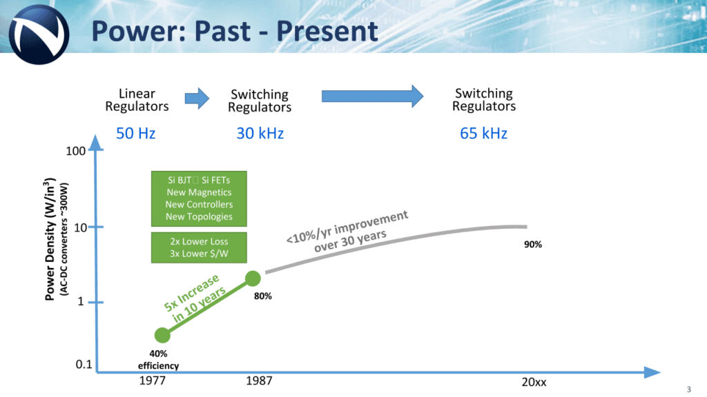
The first revolution in power started in the late 1970’s with the change from silicon bipolar to silicon MOSFETs – or ‘HEXFET’ as introduced by International Rectifier (IR). At the same time, new ‘integrated’ controllers and magnetic materials enabled breakthrough topologies to advance from academia to industry, and we saw a huge increase in efficiency and frequency which drove down size and cost. Since then, the silicon world has evolved slowly, with more and more effort for smaller and smaller returns. Navitas was founded in 2014, at a time when power gallium nitride (GaN) had almost crossed the bridge from academia to proven industrial release.
Many members of the original management team had worked together at IR, and with the catalyst of UCSB materials talent, “got the band back together” to learn from the mis-steps of the past – dMode, cascoding, discretes with high-inductance packaging – and leap ahead with eMode, integration and frequency-optimized packaging.
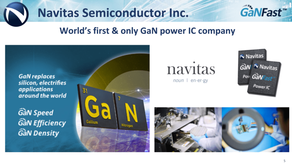
Navitas means ‘energy’ and our focus is on energy savings and bringing a new level of energy to power electronics. By exploiting the inherent high-speed performance of GaN – specifically as the world’s first GaN power IC company – we can drive efficiencies and power densities to new levels.
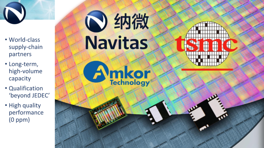
After early work at the Hughes Research Laboratory (HRL) – and working out of a trailer in the parking lot – we looked for a platform closer to industrial qualification, and partnered with TSMC for wafers and Amkor for packaging. They are outstanding, world-class supply-chain partners and we are confident in their ability and commitment to support the dramatic growth expectations we have for our GaN power ICs
It took some cycles of learning and a new, higher-level, Navitas-proprietary AllGaN™ process design kit to achieve a robust design. That PDK is the key to GaN’s successful attack on silicon – true, monolithic integration – combining GaN FET, GaN logic and GaN analog circuits to achieve a ‘digital-in, power-out’ MHz building block.
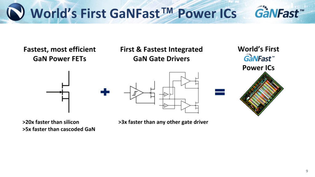
Monolithic integration enables high-frequency power conversion and the ability to shrink passive components like transformer, EMI filters, output capacitors – to deliver solutions that can charge 3x faster in half the size and weight of old, slow, silicon solutions.
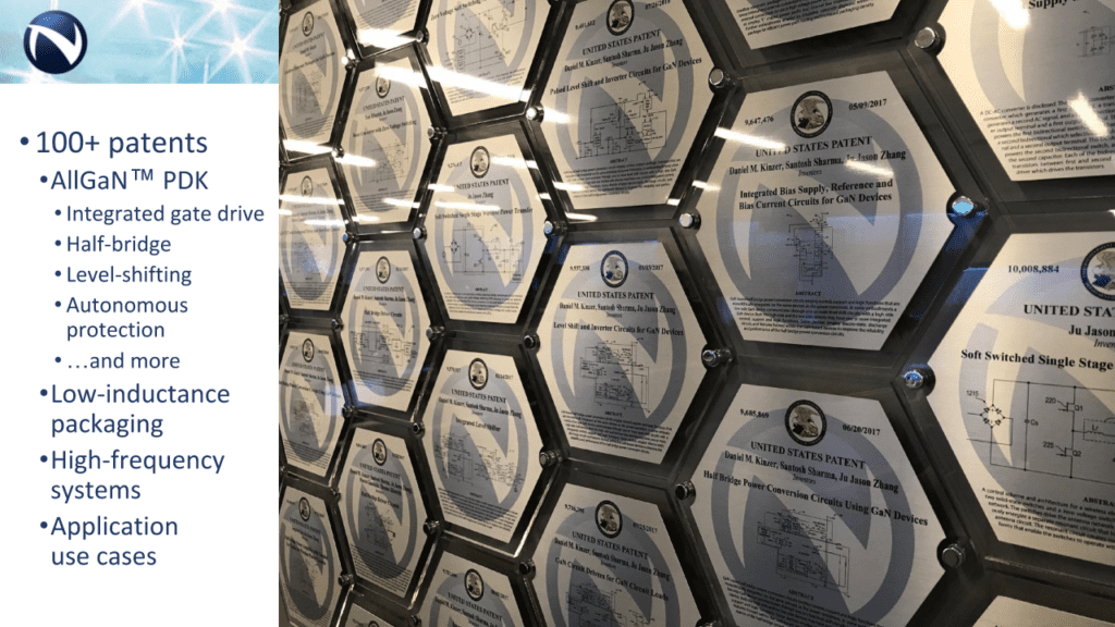
The pace of innovation is increasing – with further integration and higher-level functions to improve the performance and reliability of next-generation power systems.
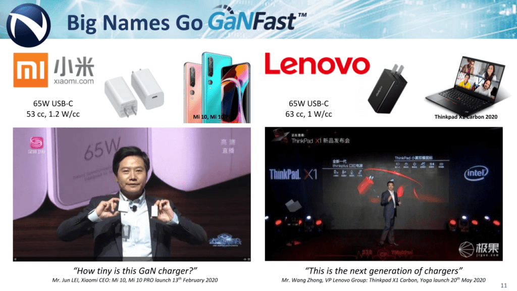
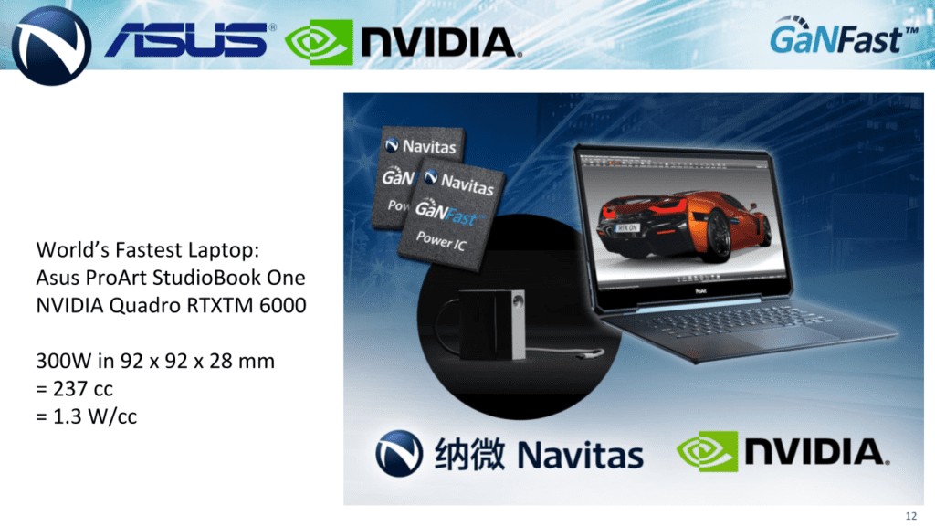
The market for next-generation fast chargers is US$1B today, with a rapid adoption of GaN. For Xiaomi and Lenovo, the world’s smallest 65W chargers have been released at retail prices 50-75% lower than previous best-in-class silicon chargers. At higher power, Navitas worked closely with Asus & NVIDIA to deliver the world’s smallest 300W supply for the world’s fastest laptop.
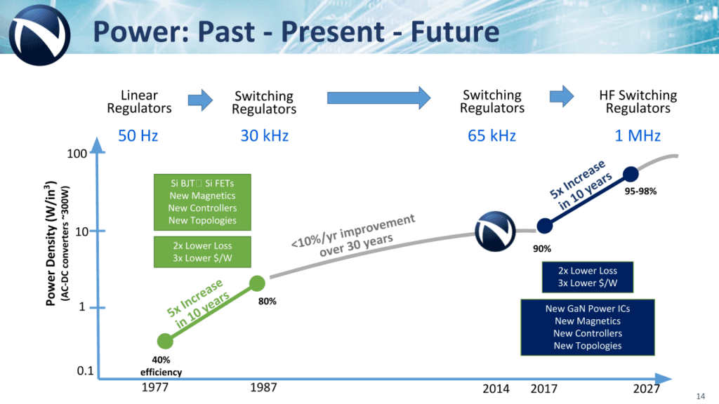
40 years on, the same revolutionary factors – a new material, integration, magnetics and topologies increase efficiency and frequency so driving down size and cost again.
Our roadmap is laser-focused on helping power designers to exploit the high-speed performance of GaN, and it’s all about speed. The strategy is more features, more integration, higher frequencies, new voltages, new topologies and strong partnerships with controller, magnetics, and capacitor companies in the MHz eco-system. GaN is fast, very fast and we’ll see it in all markets from fast chargers to all-in-one PCs, TVs, multi-kW server, eMobility and new energy markets.
Thank you for being part of the GaNFast community and looking to the future of GaN.


Recent Comments