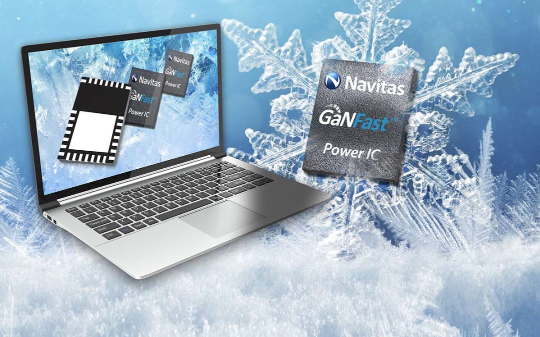
GaNFast™ power ICs are game-changers in the world of device charging. GaN-based fast chargers provide 3x more power, so charge 3x faster in half the size and weight of old, slow silicon-chip-based chargers.
GaN power ICs integrate GaN power, GaN analog and GaN logic circuits onto a single GaN chip. They run at high speeds and drastically reduce the size and cost of passive components, so more and more fast chargers are being released at 50% lower prices than comparable silicon devices when they were released.
When designers shrink fast chargers to the minimum possible size, then thermal density – or simply ‘heat’ – can be an issue.
The new NV612x-series provides a 10-15 °C reduction in temperature thanks to an advanced cooling pad to improve thermal interface to the PCB and provide a direct electrical connection to the system ground.
Not only does this enable the world’s highest power density, but it also helps designers to pass all thermal specifications and agency approvals, meaning even more manufacturers will be able to integrate it into their fast chargers, with a shorter time-to-market.
We’ve already seen some game-changing chargers from companies like Xiaomi, Belkin, OPPO and Lenovo, and this new development will see even more companies adopt gallium nitride.
GaNFast ICs are not just powering smartphones, either.
Laptops, TVs and all-in-one computers like Apple’s iMac can all benefit from GaN Power ICs. They can go even further, to multi-kW electric vehicle (EV) fast chargers plus telecom and datacenter power supplies.
Discrete GaN components – stand-alone GaN switches with exposed, vulnerable connections – require additional, complex, external driving and protection components. Integrated GaN power ICs provide a combination of simplicity and capability in one chip.
Want the fastest chargers available? Let’s Go GaNFast!

It’s good but still has long way to go for real production. For fabless companies, it’s really hard to improve some GaN device issues.
Hello Mr. Shih, thank you for comment. GaNFast power ICs entered mass production in March 2018. TSMC is our world-class wafer partner. Over 5,000,000 have been shipped with zero failures. Regards, Steve.