
by Navitas | May 28, 2024 | Short post, Tech Features
“Belkin is a well-known accessories brand, with chargers, data cables, wireless chargers, converters and other accessories. Charging Head Network has obtained the BoostCharge Pro USB-C 4-port gallium nitride charger launched by Belkin. This charger model is...
by Navitas | Apr 15, 2024 | Front Page, In the Media, Latest News, Short post, Tech Features
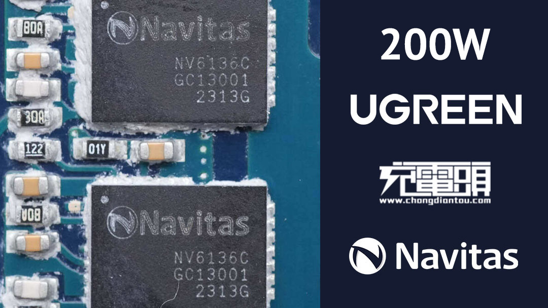
“Ugreen has launched a smart charging magic box Ultra+ with 200W output power . This product is in the form of a desktop charger. It comes with a 1.8-meter-long power cord and is equipped with two new national standard five-hole jacks to meet the needs of...
by Navitas | Nov 2, 2023 | Short post, Tech Features
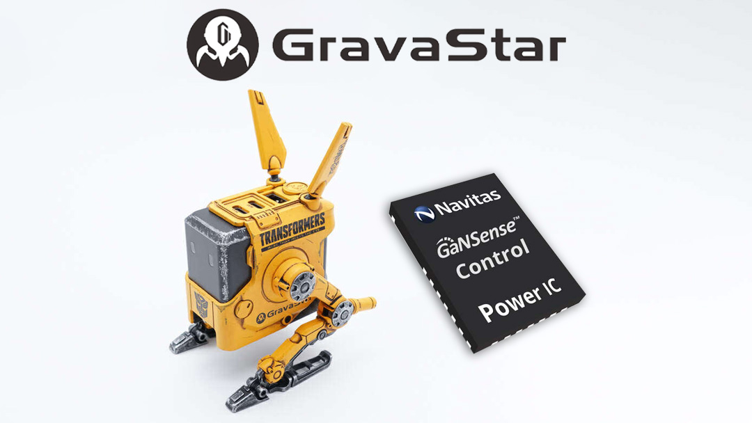
“This charger from Gravity Planet is a co-branded model of Transformers and Bumblebee. The charger shell is designed with a yellow tone and uses folding pins. The overall feel is quite good. The charger has a 2C1A interface, of which the USB-C1 interface has an...
by Navitas | Aug 25, 2023 | Short post, Tech Features
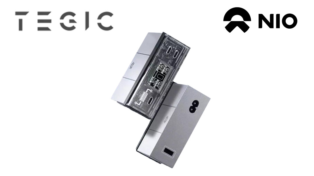
“In 2021, TEGIC, a company that focuses on high-performance fast charging accessories, collaborated with NIO to launch a customized 90W GaN power station, which brought a high-power portable experience to NIO car owners. Recently, TEGIC and NIO have launched...
by Navitas | Aug 3, 2023 | Short post, Tech Features
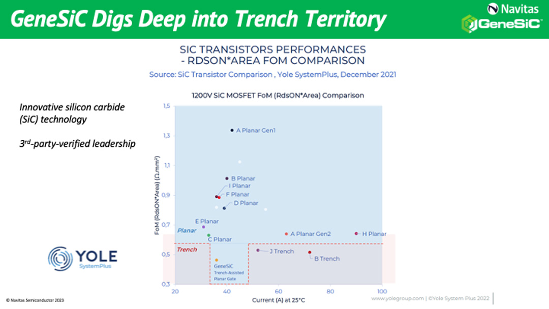
Yole Group’s SiC MOSFET Comparison Report, covers 37 SiC transistors, demonstrating GeneSiC’s unique ‘Trench-Assisted Planar-Gate’ technology, with the lowest FoMs in the industry! GeneSiC offers a no-compromise, next-generation solution;...

by Navitas | Feb 16, 2023 | Short post, Tech Features
Spigen’s ArcStation™ Pro 20W Wall Charger is engineered with Navitas’ GaNFast™ technology that allows the ArcStation to be 30% smaller than the standard 18W iPhone charger. ‘The charger is based on Gallium Nitride (GaN) technology, which is a big...

Recent Comments