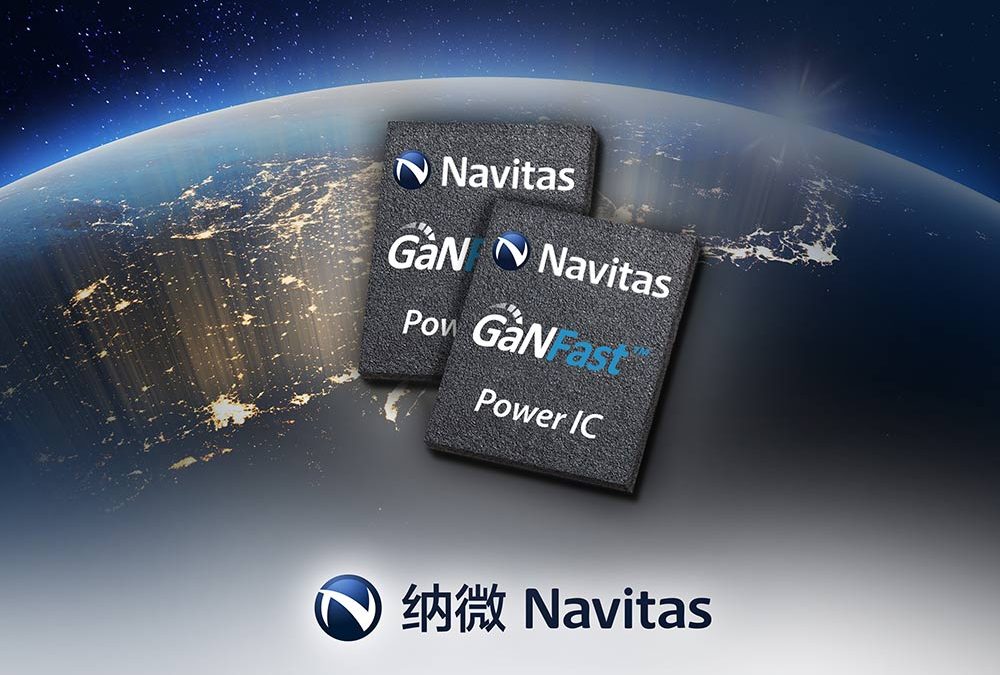
World-class, state-of-the-art knowledge and collaboration for a new class of high-frequency, high-efficiency, high-density power systems
EL SEGUNDO, Calif.–(PRWeb)— Navitas Semiconductor today announced the opening of a new GaNFast Design Center, in Hangzhou, China, to enable pioneering partner customers to deliver leading edge converter designs that are 50% smaller, 50% lighter and can charge mobile applications up to 3x faster than old, slow silicon-based designs.
“The GaNFast Design Center is staffed with experienced, proven, high-level application engineers, chartered to develop new high-frequency, high-efficiency and high density power systems, and to assist customers to exploit fully the key performance and benefits of GaNFast power ICs.” said Michael Xu, Sr. Director of Applications and head of the new facility. “We have the tools, skills and resources to develop new, advanced power architectures, and simultaneously ensure customers meet all critical specifications, from efficiency and thermal optimization to EMI compliance for mass production”.
The world’s first GaNFast power ICs enable simultaneous MHz-frequency and highest-efficiency operation. These advances translate to smaller, lighter, lower system cost power conversion in mobile fast chargers and adapters, LED TVs, EV/Hybrid, LED lighting and new energy solutions.
“The Hangzhou location is central to China’s academic & innovation hub, with very close links to Zhejiang University and customers’ advanced research locations in Shanghai and Suzhou,” said Dan Kinzer, Navitas CTO, adding “Navitas’ vision is to exploit GaN power IC performance to create a new class of high-frequency, high-efficiency, high-density power systems”.
The opening ceremony features a welcome presentation by Navitas CEO, Gene Sheridan, who added, “Following the recent Navitas Shenzhen opening, the new Hangzhou GaNFast Design Center shows significant investment in technical advances and strong customer support in China. Through semiconductor, and system-level innovations, combined with industry partnerships, we can transform this RMB 200B/year industry.”
About Navitas:
Navitas Semiconductor Inc. is the world’s first and only GaN Power IC company, founded in 2014 and based in El Segundo, CA, USA. Navitas has a strong and growing team of power semiconductor industry experts with a combined 200 years of experience in materials, devices, applications, systems and marketing, plus a proven record of innovation with over 200 patents among its founders. A proprietary process design kit monolithically integrates the highest performance GaN FETs with GaN logic and GaN analog circuits. Navitas GaNFast™ Power ICs enable smaller, higher energy efficient and lower cost power for mobile, consumer, enterprise and new energy markets – over 35 Navitas patents are granted or pending.
###
Navitas Semiconductor, GaNFast and related logos are trademarks or registered trademarks of Navitas Semiconductor, Inc. All other brands, product names and marks are or may be trademarks or registered trademarks used to identify products or services of their respective owners.

Recent Comments